参考手册
| 本手册正在修订中,以涵盖KiCad的最新稳定发布版本。 它包含一些内容尚未编写完成。 我们希望您能耐心等待我们的志愿技术作者完成这项工作。 同时我们也欢迎新的贡献者加入我们的行列,帮助我们使 KiCad 的文档比以前更好。 |
版权
This document is Copyright © 2010-2024 by its contributors as listed below. You may distribute it and/or modify it under the terms of either the GNU General Public License (http://www.gnu.org/licenses/gpl.html), version 3 or later, or the Creative Commons Attribution License (http://creativecommons.org/licenses/by/3.0/), version 3.0 or later.
本指南中的所有商标均属于其合法所有者。
贡献人员
Jean-Pierre Charras, Fabrizio Tappero, Wayne Stambaugh, Cirilo Bernardo, Jon Evans, Graham Keeth
翻译人员
Qinghan Hu <[email protected]>, 2023.
taotieren <[email protected]>, 2019-2023.
Telegram 简体中文交流群: https://t.me/KiCad_zh_CN
译者注:英文双引号包含的中文为软件的功能操作。
反馈
The KiCad project welcomes feedback, bug reports, and suggestions related to the software or its documentation. For more information on how to submit feedback or report an issue, please see the instructions at https://www.kicad.org/help/report-an-issue/
KiCad PCB 编辑器简介
初始配置
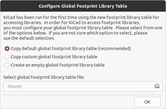
当 PCB 编辑器第一次运行时,如果在 KiCad 配置文件夹中没有找到全局封装表文件 fp-lib-table,那么 KiCad 将询问如何创建这个文件:
第一个选项是推荐的(复制默认的全局封装库表)。默认的封装库表包括所有作为 KiCad 的一部分安装的标准封装库。
如果该选项被禁用,KiCad 无法找到默认的全局封装库表。这可能意味着你没有和 KiCad 一起安装标准封装库,或者它们没有被安装在 KiCad 期望找到的地方。在某些系统中,KiCad 库是作为一个单独的软件包安装的。
-
如果你已经安装了标准的 KiCad 封装库并想使用它们,但第一个选项被禁用,选择第二个选项并浏览到安装 KiCad 库的目录中的
fp-lib-table文件。 -
如果你已经有了一个你想使用的自定义封装库表,选择第二个选项并浏览到你的
fp-lib-table文件。 -
如果你想从头开始构建一个新的封装库表,选择第三个选项。
封装库的管理 之后 有更详细的描述。
PCB 编辑器的用户界面
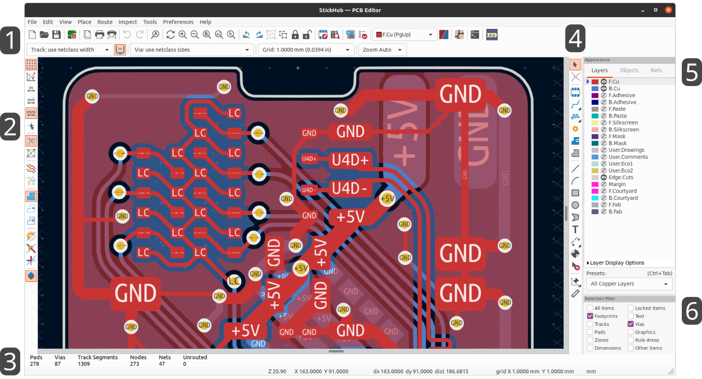
PCB 编辑器的主要用户界面如上图所示,并标明了一些关键元素:
-
顶部工具栏 (文件管理、缩放工具、编辑工具)
-
左侧工具栏 (显示选项)
-
消息面板和状态栏
-
右侧工具栏 (绘图和设计工具)
-
外观面板
-
选择过滤器面板
浏览编辑画布
编辑画布是正在设计的电路板视图。您可以平移和缩放到电路板的不同区域,也可以翻转视图以从底部显示电路板。
默认情况下,用鼠标中键或右键拖动会平移画布视图,滚动鼠标滚轮会放大或缩小视图。 你可以在偏好设置中的鼠标和触摸板部分改变这一行为(详见 配置和定制)。
在顶部的工具栏中,还有其他几个缩放工具可用:
-
 放大视口的中心。
 -
 从视口中心缩小。
 -
 缩放以适应绘图页周围的框架。
 -
 缩放以适应绘图页内的对象。
 -
 允许你画一个方框来确定缩放的区域。
光标的当前位置显示在窗口的底部(X 和 Y),同时显示的还有当前的缩放系数(Z)、光标的相对位置(dx、dy 和 dist)、网格设置和显示单位。
按 Space 可以将相对坐标重置为零。这对于测量两点之间的距离或对齐对象很有用。
快捷键
快捷键 Ctrl+F1 显示当前快捷键列表。默认的快捷键列表包含在本手册的 Actions Reference 部分。
本手册中描述的快捷键使用了标准 PC 键盘上的按键标签。在苹果键盘布局中,使用 Cmd 键来代替 Ctrl,使用 Option 键来代替 Alt。
许多操作默认没有分配快捷键,但可以使用快捷键编辑器(偏好设置 → 偏好设置… → 快捷键 )分配或重新定义快捷键。
| 通过快捷键可用的许多操作也可在上下文菜单中使用。要访问上下文菜单,请在编辑画布中单击鼠标右键。根据选择的内容或处于活动状态的工具,将提供不同的操作。 |
快捷键存储在 KiCad 的配置目录下的 user.hotkeys 文件中。这个位置是特定于平台的:
-
Windows:
%APPDATA%\kicad\8.0\user.hotkeys -
Linux:
~/.config/kicad/8.0/user.hotkeys -
macOS:
~/Library/Preferences/kicad/8.0/user.hotkeys
KiCad 可以使用快捷键编辑器中的 导入快捷键 按钮从 user.hotkeys 文件中导入快捷键设置。
显示和选择控件
板层
PCB 编辑器中的层代表电路板上的物理铜层,以及用于定义丝印、阻焊和电路板边框等的图形层。 在编辑器中,总有一个层是活动的。 活动图层绘制在其他图层之上,并将成为分配给新创建对象的图层。 活动层在顶部工具栏的图层选择器下拉框中显示,在外观面板中也被突出显示。 要改变活动层,你可以左键单击外观面板中的层名,使用顶部工具栏中的下拉层选择器,或使用快捷键。 图层可以被隐藏以简化电路板视图。 你可以隐藏一个层,即使它是活动层。
电路板层的显示顺序
The display order for board layers is dynamic and depends on which layer is selected as the active layer. The active layer is always drawn on top of other layers. In addition, layers that are related to the active layer are drawn on top of layers that are unrelated. For example, if you make B.Silkscreen the active layer, then all of the other back layers (B.Cu, B.Adhesive, B.Paste, B.Mask, B.Fab, and B.Courtyard) will be drawn on top of the front, user, and inner copper layers, with B.Silkscreen topmost. If you make Edge.Cuts active, then it will be drawn on top, and the User.* layers and Margin will also be be brought to the front.
| Selected objects are always drawn on top, even if they are not on the active layer. |
外观面板
外观面板提供了管理 PCB 编辑器绘图画布中的对象的可见性、颜色和不透明度的控制。 它有三个标签:层标签包含电路板层的控制,对象标签包含不同类型图形对象的控制,网络标签包含飞线和铜对象的外观控制。
图层控件
在外观面板的 “层” 选项卡中,每个电路板层都显示了其颜色和可见性状态。 活动层在色块的左边有一个箭头指示器。 左键点击一个图层来选择它作为活动图层。 左键单击相应的可见性图标,在可见和隐藏之间切换该图层。 双击或中击色块来改变该图层的颜色。
| 必须先在偏好选项中创建自定义颜色主题, 然后才能在“外观”面板中更改图层颜色。 |
在图层列表下方是一个包含图层显示选项的可展开面板。第一个设置控制非活动图层的显示方式:正常、暗显或隐藏。层显示模式可用于简化视图并聚焦于单个层。当非活动层显示模式为 "暗显" 或 "隐藏" 时,不能选择非活动层上的对象。您可以使用快捷键 Ctrl+H 快速切换这些显示模式。
翻转电路板视图 将显示电路板,就像从底部看一样(即绕 Y 轴镜像)。 此选项也可在视图菜单中使用。
| 翻转电路板视图不会更改可视层顺序,活动层将保持在最前面,其他层按正常顺序紧随其后。 |
对象控件
外观面板的 "对象" 选项卡与 "图层" 选项卡类似。 主要区别在于,有些对象没有颜色设置,而四种类型的对象(布线、过孔、焊盘和敷铜)有不透明度控制滑块。 这里的不透明度设置将与图层颜色中设置的任何不透明度相乘。 默认情况下,所有对象都是完全不透明的,除了敷铜,敷铜被设置为半透明,以便通过敷铜区域更容易看到对象。
图层预设
图层预设存储了哪些图层和对象是可见和隐藏的,以便于调用。 有几个内置的图层预设,您也可以保存您自己的自定义预设。 自定义预设存储在一个电路板的工程设置中,因为预设可能是特定于某个电路板的层叠。
要加载一个预设,请从外观面板底部的预设下拉菜单中选择它,或者通过按住 Ctrl 并按 Tab 来使用快速切换器。 一旦快速切换器窗口出现,你可以按 Tab 和 Shift+Tab 来循环浏览可用的预设。 当你放开 Ctrl 键时,高亮显示的预设将被加载。
To save a custom preset, first use the visibility controls to choose which layers you want visible, then choose Save preset… from the Presets drop-down menu. Give your preset a name and it will now be available via the drop-down menu and the quick switcher. To modify a custom preset, follow the same process and save the modified version with the same name to overwrite the existing version. To delete a custom preset, choose the Delete preset… option from the drop-down menu and select the preset to be deleted from the list.
Viewports
Viewports store the current view location and zoom level so you can quickly switch back to it later, or switch between several saved views.
To load a viewport, choose it from the Viewports drop-down menu at the bottom of the appearance panel or use the quick switcher by holding down Shift and pressing Tab. Once the quick switcher window appears, you can press Tab to cycle through the stored viewports. When you let go of the Shift key, the highlighted viewport will be loaded.
To save a new viewport, scroll and zoom to show the desired area of the board, then choose Save viewport… from the Viewports drop-down menu. Give your viewport a name and it will now be available via the drop-down menu and the quick switcher. To modify an existing viewport, save a new viewport with the same name to overwrite the existing version. To delete a viewport, choose the Delete viewport… option from the drop-down menu and select the preset to be deleted from the list.
网络和网络类控件
外观面板的网络选项卡显示电路板中所有网络和网络类的列表。每个网络都有一个可见性控件,用于控制该网络在飞线中的可见性。在飞线中隐藏网络不会改变电路板的连接性,也不会影响设计规则检查器;这只是为了使飞线更容易理解。
每个网络和网络类还可以指定一种颜色。默认情况下,此颜色适用于网络 (或网络类中的所有网络) 的飞线。默认情况下,网络没有颜色;这由色样中的棋盘格图案指示。双击或右键单击网络或网络类颜色样本以设置颜色。
| 默认网络类不能分配颜色, 因为该类中的网络将仅使用颜色主题定义的默认飞线颜色。 |
您还可以通过外观面板选择并高亮网络和网络类:右击网络或网络类以在菜单中显示这些选项。
网络类列表下面是一个包含网络显示选项的可扩展面板。第一个选项控制如何应用网络颜色。当选择了 “所有” 时,属于网络或网络类的所有铜对象 (焊盘、布线、过孔和敷铜) 都将呈现所选的颜色。当选中 “飞线” (默认值)时,只有飞线受网络和网络类颜色的影响。 当选择 “无” 时,网络和网络类颜色被忽略。
第二个选项控制如何绘制飞线。“所有图层” 表示将在所有未连接的项目之间绘制飞线。“可见层” 意味着不会向隐藏层上的项目绘制任何最新的飞线,即使这些项目是未连接的。
| You can configure the thickness of ratsnest lines in the PCB Editor Editing Options section of the Preferences dialog, to make the ratsnest more or less visible. |
选择和选择筛选器
选择编辑画布中的对象是用鼠标左键完成的。 单独点击一个对象将选择该对象,而拖动将执行框选。 从左到右的框选将只选择完全在框内的对象。 从右到左的方框选择将选择任何接触到方框的对象。从左到右的选择框是用黄色画的,光标表示排他性选择,从右到左的选择框是用蓝色画的,光标表示包容性选择。
可以通过在单击或拖动的同时按住快捷键来修改选择操作。单击以选择单个对象时,将应用以下快捷键:
| 修改键 (Windows) | 修改键 (Linux) | 修改键 (macOS) | 选择效果 |
|---|---|---|---|
Ctrl |
Ctrl |
Cmd |
切换选择。注意:Ctrl+点击可以被重新设置为高亮网络。 偏好设置 → PCB 编辑器 → 编辑选项. |
Shift |
Shift |
Shift |
将该对象添加到现有的选择中。 |
Ctrl+Shift |
Ctrl+Shift |
Cmd+Shift |
从现有的选择中删除对象。 |
长点击 |
长点击或 Alt |
长点击或 Option |
从弹出式菜单中澄清选择。 |
拖动以执行选框时,将应用以下快捷键:
| 修改键 (Windows) | 修改键 (Linux) | 修改键 (macOS) | 选择效果 |
|---|---|---|---|
Ctrl |
Ctrl |
Cmd |
切换选择。 |
Shift |
Shift |
Shift - Shift |
将对象添加到现有的选择中。 |
Ctrl+Shift |
Ctrl+Shift |
Cmd+Shift |
从现有选择中删除对象。 |
PCB 编辑器窗口右下角的选择过滤器面板控制哪些类型的对象可以用鼠标选择。 关闭不需要的对象类型的选择,可以使在密集的电路板上选择项目更加容易。 "所有项目" 复选框是打开和关闭其他项目的一个快捷方式。 "锁定的项目" 复选框与其他项目无关,它控制是否可以选择被锁定的项目。 你可以右键单击选择过滤器中的任何对象类型,快速改变过滤器,只允许选择该类型的对象。
当一个连接的铜对象被选中时,你可以使用右键菜单中的 "扩展选择" 命令或快捷键 U 将选择扩展到同一网络的其他铜线对象。 第一次运行这个命令时,选择将被扩展到最近的焊盘。 第二次,选择将被扩展到所有层上的所有连接项。
选择一个对象会在窗口底部的信息面板上显示该对象的信息。双击一个对象可以打开一个窗口来编辑该对象的属性。
按 Esc 将始终取消当前工具或操作,并返回到选择工具。在选择工具处于活动状态时按 Esc 将清除当前选择。
网络高亮
电气网络(或一组网络)可以在 PCB 编辑器中被高亮显示,以显示该网络是如何在 PCB 上布线的。 通过在 PCB 编辑器中选择要高亮的网络,或者在启用交叉探测高亮时在原理图编辑器中选择相应的网络,可以激活网络的高亮(见下文)。 当网络高亮激活时,高亮的网络将以较亮的颜色显示,所有其他对象将以比正常颜色更暗的颜色显示。
There are three ways to select a net or nets to highlight in the PCB editor: by using the hotkey ` after selecting a copper object, by using the context menu of any copper object, and by using the context menu of the Nets tab of the Appearance panel. When you press the Highlight Net hotkey, the nets of any selected copper items will be highlighted. If no copper items are selected, the net of the copper item under the editor cursor will be highlighted.
网络高亮可以通过使用清除网络高亮动作(快捷键 ~)或在原理图中的一个空区域使用高亮网络工具来清除。 默认情况下,Esc 也会清除网络高亮,但如果需要,可以在偏好 → PCB编辑器 → 编辑选项中禁用。
选择一个或多个网络进行高亮时,左侧工具栏上的切换网络高亮显示操作将被激活(也可通过快捷键 Ctrl+` 访问)。此操作将打开或关闭高亮,而无需选择要高亮的新网络。
从原理图交叉探测
KiCad 允许在原理图和 PCB 之间进行双向交叉探测。 有几种不同类型的交叉探测。
Selection cross-probing allows you to select a symbol or pin in the schematic to select the corresponding footprint or pad in the PCB (if one exists) and vice-versa. By default, cross-probing will result in the display centering on the cross-probed item and zooming to fit. You can disable the centering and zooming behavior, or disable selection cross-probing entirely, in the Display Options section of the Preferences dialog. Even when selection cross-probing is disabled, you can manually cross-probe from the schematic to the PCB by right-clicking an object and selecting Select on PCB, or from the PCB to the schematic by right-clicking an object and choosing Select → Select on Schematic.
高亮交叉探测 允许您同时高亮原理图和 PCB 中的网络。 如果在偏好设置对话框的显示选项部分中启用了选项 "高亮交叉网络", 则在原理图编辑器中高亮某个网络或总线将导致相应的一个或多个网络在 PCB 编辑器中高亮。
左侧工具栏显示控件
左侧的工具栏提供了改变 PCB 编辑器中对象显示的选项。
|
Turns grid display on/off. Note: by default, hiding the grid does not disable grid snapping. This behavior can be changed in the Display Options section of Preferences. |
|
Turns item-specific grid overrides on/off. |
|
Switch between polar and Cartesian coordinate display in the status bar. |
|
Display/entry of coordinates and dimensions in inches, mils, or millimeters. |
|
Switches between full-screen and small editing cursor (crosshairs). |
|
Switches between free angle and 45 degree mode for placement of new tracks, zones, graphical shapes, dimensions, and other objects. You can also toggle between free angle and 45 degree mode using Shift+Space. |
|
Turns the ratsnest display on/off. |
|
Switches between straight and curved ratsnest lines. |
|
Switches the non-active layer display mode between Normal and Dim. Note: this button will be highlighted when the non-active layer display mode is either Dim or Hide. In both cases, pressing the button will change the layer display mode to Normal. The Hide mode can only be accessed via the controls in the Appearance Panel or via the hotkey Ctrl+H. |
|
When a net has been selected for highlighting, switches the highlighting on or off. Note: this button will be disabled when no net has been highlighted. To highlight a net, use the hotkey `, right-click any copper object in the net and choose Highlight Net from the Net Tools menu, or right-click the net in the list in the Nets tab of the Appearance panel. |
|
Show zone filled areas. |
|
Show zone outlines only. |
|
Switches display of pads between filled and outline mode. |
|
Switches display of vias between filled and outline mode. |
|
Switches display of tracks between filled and outline mode. |
|
Shows or hides the Appearance and Selection Filter panels on the right side of the editor. |
|
Shows or hides the Properties Manager panel on the left side of the editor. |
创建 PCB
PCB 的基本概念
KiCad 中的印刷电路板通常由代表电子元件及其焊盘的 封装、定义这些焊盘如何彼此连接的 网络、形成每个网络中焊盘之间的铜连接的 布线、过孔 和 敷铜 以及定义电路板边缘、丝印标记和任何其他所需信息的各种图形形状组成。
KiCad 通常会将 PCB 上的网络信息与相关的原理图保持同步,但也可以直接在 PCB 编辑器中创建和编辑网络。
性能
KiCad 能够创建多达 32 个铜层、14 个技术层 (丝印、阻焊、元件粘合剂、锡膏等) 和 13 个通用绘图层的印刷电路板。
KiCad 中所有对象的内部测量分辨率为 1 纳米,测量值以 32 位整数存储。 这意味着可以创建最大约 4 米乘 4 米的电路板。
KiCad 目前支持每个工程/原理图一个电路板文件。
从原理图开始
从原理图创建电路板是 KiCad 的推荐工作流程。 当您创建一个新工程时,KiCad 会生成一个与工程名称相同的空板文件。 要在创建原理图后开始设计电路板,只需打开电路板文件。 您可以通过 KiCad 工程管理器,或者点击原理图编辑器中的 "在电路板编辑器中打开 PCB" 按钮来完成。 要将原理图设计信息导入电路板编辑器,包括封装和网络连接,请使用 工具 → 从原理图更新PCB… 操作(F8)。你也可以使用顶部工具栏上的 ![]() 图标。
图标。
| 从原理图更新 PCB 是将设计信息从原理图转移到 PCB 的首选方法。在旧版本的 KiCad 中,相应的过程是将网表从原理图编辑器中导出并导入到电路板编辑器中。现在已经没有必要使用网表文件了。 |
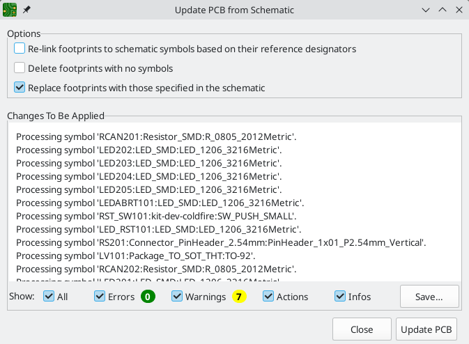
关于从原理图更新PCB工具的更多信息,请参见手册的 [正向批注,正向批注] 部分。
从头开始
也可以创建一个没有匹配原理图的电路板,不过这种工作流程有一些限制,不建议大多数用户使用。为此,您必须独立启动 PCB 编辑器(而不是从 KiCad 工程管理器启动)。在开始设计之前,最好先保存电路板文件,这也将创建一个项目文件来存储电路板设置。 使用文件菜单中的 "另存为… " 来选择保存电路板文件的位置。一个具有相同名称的项目文件将被创建在你选择保存电路板文件的相同位置。
电路板设置
在开始设计电路板之前,使用电路板设置对话框来配置电路板的基本参数。要打开电路板设置,请单击顶部工具栏中的 ![]() 图标或从文件菜单中选择 "电路板设置…"。
图标或从文件菜单中选择 "电路板设置…"。
配置电路板层叠和物理参数
在 "电路板设置" 中,有两个部分用于配置电路板的层叠和层。 "电路板编辑器层" 部分用于启用或禁用技术层(非铜层),如果需要的话,还可以给各层自定义名称。 物理层叠部分用于配置铜层的数量,以及铜层和电介质层的物理参数,如厚度和材料类型。介电层、阻焊层和丝印层可以被分配颜色,这将影响电路板在 3D 查看器中的外观。
要配置电路板的层叠,从物理层叠部分开始:
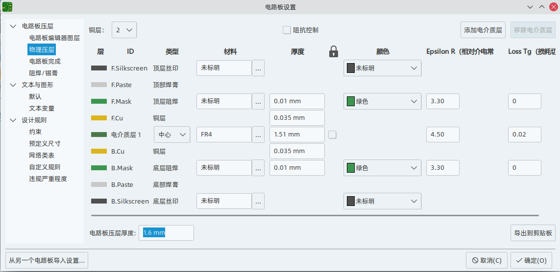
Set the number of copper layers in the upper left corner and then enter the physical parameters of the stackup if desired. These parameters may be left at their default values, but note that the board thickness value will be used when exporting a 3D model of the board, and layer thicknesses will be included in net length calculations for any nets that include vias. If you plan to use these features, it is a good idea to ensure that the stackup thickness is correct.
| KiCad 目前仅支持铜层数为偶数的层叠。 要创建具有奇数层的设计 (例如,柔性印刷电路板或金属芯印刷电路板), 只需选择下一个最高的偶数,而忽略多余的层。 |
接下来,如果需要,可以使用电路板编辑器层部分重命名或隐藏您不会在设计中使用的非铜层。例如,如果您不打算在设计中使用底层丝印,请取消选中 B.Silkcreen 层旁边的复选框。
| 在电路板编辑器层部分,可以将铜层指定为信号层、电源层、混合层或跳线层。 本指南仅供用户参考。 无论在此对话框中将类型配置为什么,都可以在任何铜层上布线和敷铜。 |
在电路板编辑器对话框的电路板表面处理(Board Finish)和阻焊/锡膏部分可以找到一些其他的电路板层叠设置。电路板表面处理部分包含用于定义铜的表面处理和特殊功能 (如刻痕或边缘电镀) 的设置。请注意,这些设置目前只影响作为 Gerber 文件一部分的电路板属性输出。
阻焊/锡膏部分允许全局调整电路板上焊盘的铜形和阻焊/锡膏形之间的间隙(正或负)。 这些值将被添加到在个别封装或焊盘上设置的任何间隙覆盖。 正的间隙值将导致阻焊层或锡膏开口的形状比铜的形状 更大。 负的间隙值将导致开口比铜的形状 更小。
| 大多数商业 PCB 制造商希望这些值为零,并在 CAM 过程中自行调整阻焊和锡膏开口。 通常最好将这些值保留为默认值零, 除非您自己制作 PCB, 或者您的制造商有具体建议使用不同的值。 |
配置默认文本和图形设置
电路板设置对话框的文本和图形默认值部分可用于配置将用于放置在电路板上的新文本和图形形状的属性。
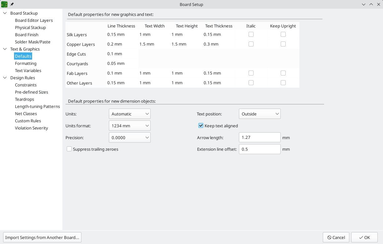
可以为对话框中显示的六种不同类别的图层配置线粗细、文本大小和文本外观。此外,可以为所有图层配置标注对象的特性。有关标注属性的更多详细信息,请参阅下面的标注部分。
虚线的外观是在 "格式化" 部分控制的。虚线长度 控制虚线的长度,而 间隔长度 控制虚线和圆点之间的间距。虚线和间隔的长度是相对于行宽而言的:间隔长度为 2 意味着是行宽的两倍。
文本替换变量可以在文本变量部分创建。 这些变量允许你将变量名称替换为任何文本字符串。 这种替换发生在变量名称在 ${VARIABLENAME} 的变量替换语法内的任何地方。
例如,您可以创建一个名为 VERSION 的变量,并将文本替换设置为 1.0。 现在,在 PCB 上的任何文本对象中,你可以输入 ${VERSION},KiCad 将替代 1.0。 如果你把变量改为 2.0,每个包括 ${VERSION} 的文本对象都会自动更新。 你也可以混合使用普通文本和变量。 例如,你可以创建一个文本对象,内容为 版本:${VERSION},它将被替换为 版本:1.0。
文本变量也可以在 原理图设置 中创建。 文本变量是项目范围内的;在原理图编辑器中创建的变量在电路板编辑器中也可用,反之亦然。
还有一些 内置系统文本变量。
配置设计规则
设计规则控制交互式布线器的行为、敷铜和设计规则检查器。设计规则可以随时修改,但我们建议您在电路板设计过程开始时建立所有已知的设计规则。
约束
基本设计规则是在电路板设置对话框的 “约束” 部分中配置。 这一部分的约束条件适用于整个板子,应该设置为板子制造商推荐的值。 这里设置的任何最小值都是一个 绝对(absolute) 的最小值,不能被更具体的设计规则所覆盖。 例如,如果你需要电路板的一部分的铜间隙为 0.2mm,其余部分为 0.3mm,你必须在约束条件部分输入 0.2mm 的最小铜间隙,并使用网络类或自定义规则来设置较大的 0.3mm 间隙。
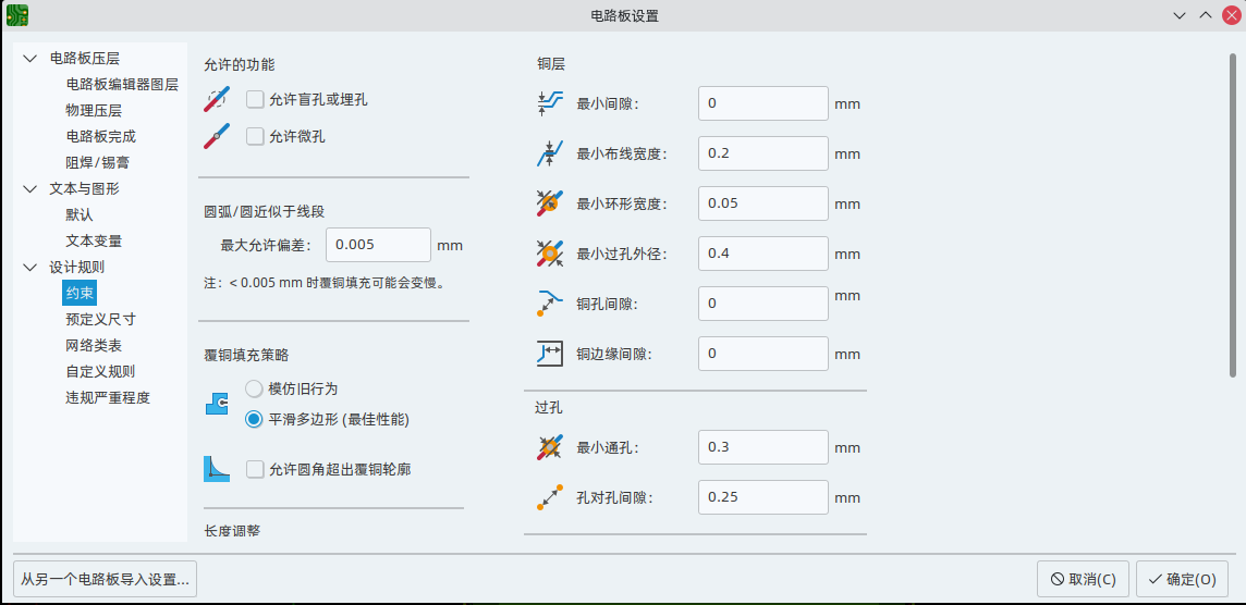
除了设置最小间隙外,还可以在此处配置许多功能:
| Setting | Description |
|---|---|
Arc/circle approximated by segments |
In some situations, KiCad must use a series of straight line segments to approximate round shapes such as those of arcs and circles. This setting controls the maximum error allowed by this approximation: in other words, the maximum distance between a point on one of these line segments and the true shape of the arc or circle. Setting this to a lower number than the default value of 0.005mm will result in smoother shapes, but can be very slow on larger boards. The default value typically results in arc approximation error that is not detectable in the manufactured board due to manufacturing tolerances. |
Allow fillets outside zone outline |
Zones can have fillets (rounded corners) added in the Zone Properties dialog. By default, no zone copper, including fillets, is allowed outside the zone outline. This effectively means that inside corners of the zone outline will not be filleted even when a fillet is configured. By enabling this setting, inside corners of the zone outline will be filleted even though this results in copper from the zone extending outside the zone outline. |
Minimum thermal relief spoke count |
This sets the minimum acceptable number of thermal relief spokes connecting a pad to a zone. A DRC violation will be generated if this constraint is violated. |
Include stackup height in track length calculations |
By default, the length tuner uses the height of the stackup to calculate the additional length of a track that travels through vias from one layer to another. This calculation relies on the board stackup height being correctly configured. In some situations, it is preferable to ignore the height of vias and just calculate the track length assuming that vias add no length. Disabling this setting will exclude via length from length tuner track length calculations. |
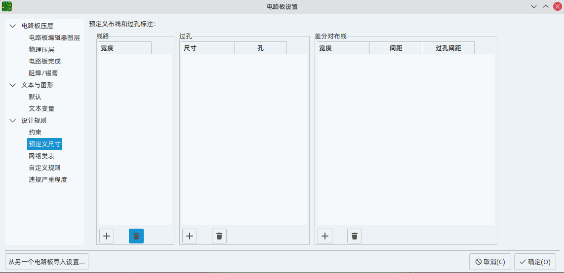
预定义大小
预定义的尺寸部分允许你定义希望在布线时可用的布线和过孔尺寸。 网络类可以用来定义不同网络中的布线和过孔的默认尺寸(见下文),但是在这个部分定义一个尺寸列表,可以让你在布线的时候在这些尺寸间切换。 例如,你可能希望电路板上的默认布线宽度是 0.2 mm,但对于一些承载更多电流的部分使用 0.3 mm,而对于一些空间有限的部分使用 0.15 mm。 您可以在电路板设置对话框中定义这些布线的宽度,然后在布线时在它们之间切换。
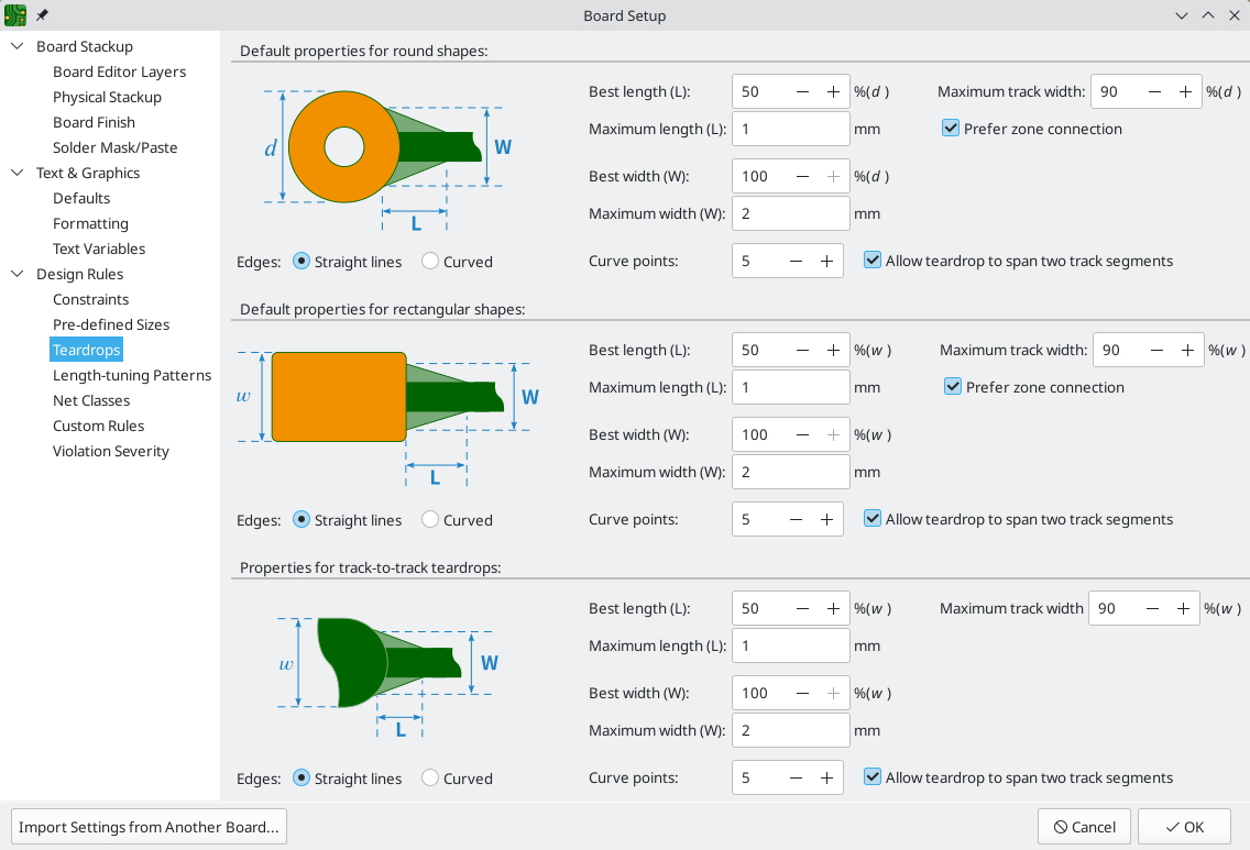
Teardrops
The teardrops section lets you set default parameters for various types of teardrops. There are different settings for teardrop connections to round objects, rectangular objects, and teardrop connections between tracks. The default teardrop parameters can be overridden when teardrops are added, and also changed in the properties for individual connected items. See the teardrops documentation for more information.
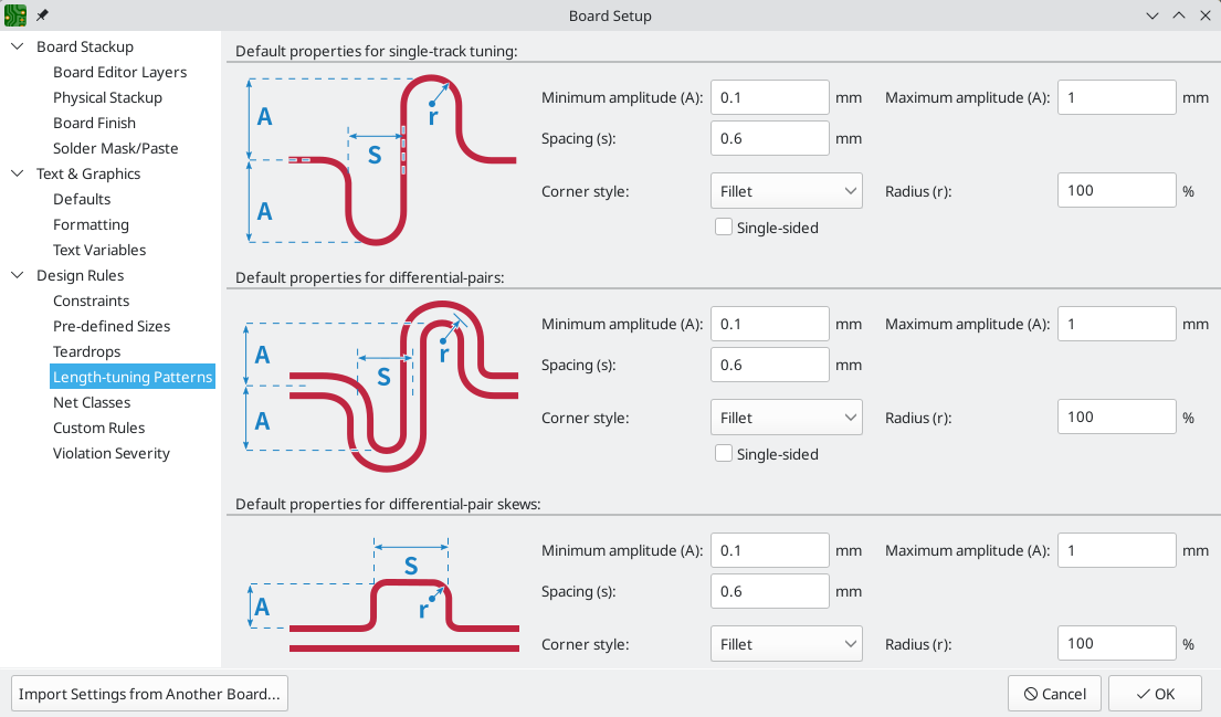
Length-tuning patterns
The length-tuning patterns section lets you set default parameters for each type of length-tuning pattern (single-track length, differential-pair length, and differential-pair skew). These defaults can be overridden in the properties of each tuning pattern added to the board. See the length tuning documentation for more ifnormation.
网络类
网络类部分允许你为不同网络类配置布线和间隙规则。 在 KiCad 中,每个网络都是某个网络类的一部分。 如果你不把网络添加到一个特定的类中,它将是默认类的一部分,总是存在。可以在原理图或电路板设置对话框中 创建和编辑网络类。
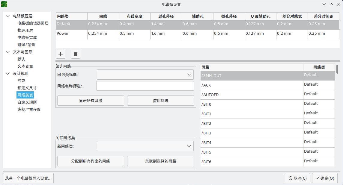
网络类部分的上部有一个表格,显示了设计中的网络类和适用于每个网络类的设计规则。 每个类别都有铜的间隙、布线宽度、过孔尺寸和差分对尺寸的值。 这些值将在创建布线和过孔时使用,除非有更具体的规则覆盖它们(见下面的自定义规则)。
任何规则都不能覆盖电路板设置的约束条件部分中设置的最小值。
例如,如果您将网络类间距设置为 0.1 mm,但约束条件部分中的最小间距设置为 0.2 mm,
则该类网络的间距将为 0.2 mm。
|
当 PCB 编辑器中的布线宽度和过孔尺寸控制设置为 "使用网络类值" 时,就会使用为每个网络类定义的布线宽度和过孔尺寸。 这些宽度和尺寸被认为是该网络类的默认或最佳尺寸。 它们不是最小或最大值。 手动将布线宽度或过孔尺寸改为与网络类部分定义的不同的值,不会导致违反 DRC。 要将布线宽度或过孔大小限制在特定的值,请使用自定义规则。
网络类部分的下半部分列出了基于模式的网络类赋值。在 原理图编辑器文档 中解释了基于模式的网络类分配的工作;基于模式的分配可以在 "电路板" 或原理图设置窗口中进行编辑。
请注意,基于模式的分配可以直接在 PCB 编辑画布上创建,方法是右击布线或敷铜并点击 分配网络类…。也可以在原理图中使用 网络类指令或标签 来分配网络类,而不是基于模式的分配。
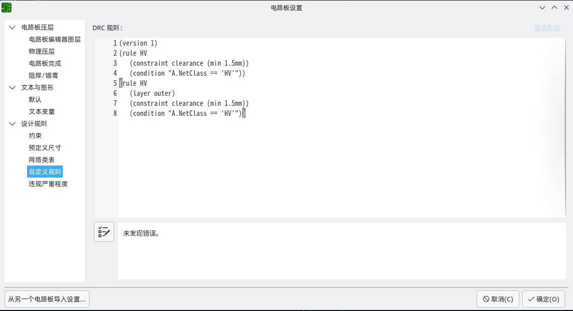
自定义规则
自定义规则部分包含一个文本编辑器,用于使用自定义规则语言创建设计规则。 自定义规则用于创建基本约束或网络类设置没有涵盖的特定设计规则检查。
只有在自定义规则定义中没有错误时,才会应用自定义规则。 在关闭电路板设置之前,使用检查规则语法器按钮来测试定义并修复任何问题。
请参阅高级主题一章中的自定义设计规则,了解关于自定义规则语言的更多信息以及规则实例。
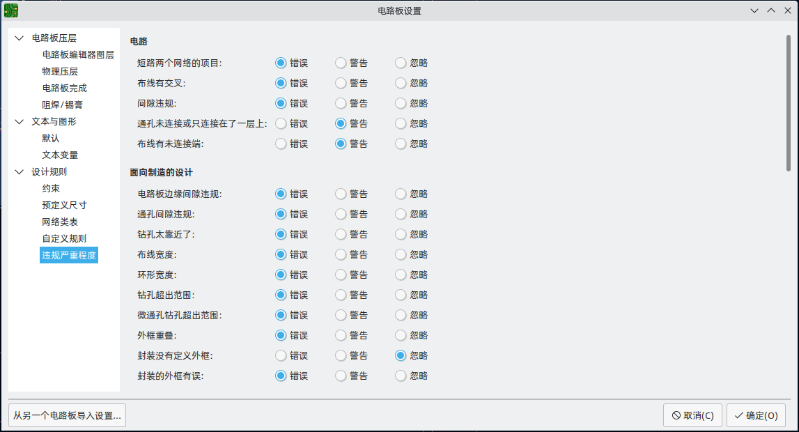
违规严重程度
违规严重性部分允许你配置每种设计规则检查的严重性。 每条规则可以被设置为创建一个错误标记、一个警告标记或没有标记(忽略)。
| 在设计规则检查器中可能会忽略个别规则违规。 在违规程度部分中将规则设置为忽略将完全禁用相应的设计规则检查。 请谨慎使用此设置。 |
导入设置
您可以从现有电路板导入部分或全部电路板设置。 这种技术可以用来创建一个 "模板" 电路板板,其中有你想在多个设计中使用的设置,然后将这些设置从模板板中导入到每个新板中,而不是手动输入。
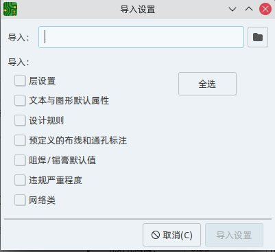
要导入设置,请点击电路板设置对话框底部的 “从另一个电路板导入设置…” 按钮,然后选择您要导入的 kicad_pcb 文件。 选择你想导入的设置,当前的设置将被选定的板子的值覆盖。
编辑电路板
放置和绘制操作
放置和绘图工具位于右侧工具栏中。 当一个工具被激活时,它将一直处于激活状态,直到选择了一个不同的工具或用 Esc 键取消该工具。 当任何其他工具被取消时,选择工具总是被激活。
某些工具栏按钮在调色板中有多个可用工具。这些工具由按钮右下角的小箭头表示:
要显示调色板,你可以在工具上点击并按住鼠标按钮,或者点击并拖动鼠标。 调色板关闭时将显示最近使用的工具。
|
Selection tool (the default tool). |
|
Local ratsnest tool: when the board ratsnest is hidden, selecting footprints with this tool will show the ratsnest for the selected footprint only. Selecting the same footprint again will hide its ratsnest. The local ratsnest setting for each footprint will remain in effect even after the local ratsnest tool is no longer active. |
|
Footprint placement tool: click on the board to open the footprint chooser, then click again after choosing a footprint to confirm its location. |
|
Route tracks / route differential pairs: These tools activate the interactive router and allow placing tracks and vias. The interactive router is described in more detail in the Routing Tracks section below. |
|
Tune length: These tools allow you to tune the length of single tracks or the length or skew of differential pairs, after they have been routed. See the Routing Tracks section for details. |
|
Add vias: allows placing vias without routing tracks. Vias placed on top of tracks using this tool will take on the net of the closest track segment and will become part of that track (the via net will be updated if the pads connected to the tracks are updated). Vias placed anywhere else will take on the net of a copper zone at that location, if one exists. These vias will not automatically take on a new net if the net of the copper zone is changed. |
|
Add filled zone: Click to set the start point of a zone, then configure its properties before drawing the rest of the zone outline. Zone properties are described in more detail below. |
|
Add rule area: Rule areas, formerly known as keepouts, can restrict the placement of items and the filling of zones and can also define named areas to apply specific custom design rules to. |
|
Draw lines. Note: Lines are graphical objects and are not the same as tracks placed with the Route Tracks tool. |
|
Draw arcs: pick the center point of the arc, then the start and end points. By right clicking this button, you can change the arc editing mode between a mode that maintains the existing arc center and a mode that maintains the arc radius. |
|
Draw rectangles. Rectangles can be filled or outlines. |
|
Draw circles. Circles can be filled or outlines. |
|
Draw graphical polygons. Polygons can be filled or outlined. Note: Filled graphical polygons are not the same as filled zones: graphical polygons cannot be assigned to a net and will not keep clearance from other items. |
|
Add bitmap image for reference. Reference images are not included in fabrication outputs. |
|
Add text. |
|
Add a textbox. |
|
Add dimensions. Dimension types are described in more detail below. |
|
Deletion tool: click objects to delete them. |
|
Set grid origin or drill/place origin (used for fabrication outputs). |
|
Interactively measure the distance between two points. |
Grids and snapping
移动、拖动和绘制电路板元素时,网格、焊盘和其他元素可以具有捕捉点,具体取决于用户偏好设置中的设置。在复杂的设计中,捕捉点可能离得太近,这会使当前的工具操作变得困难。使用下表中的快捷键可以在移动鼠标时禁用网格和对象捕捉。
| On Apple keyboards, use the Cmd key instead of Ctrl. |
| 快捷键 | 效果 |
|---|---|
Ctrl |
关闭网格捕捉。 |
Shift |
关闭对象捕捉。 |
Tools only snap to objects on visible layers. You can reduce unwanted snapping points by hiding unneeded layers or using the single-layer view mode. Additionally, you can toggle between snapping to objects on all layers or only snapping to objects on the current layer by pressing Shift+S.
Snapping to different types of objects (pads, tracks, and graphics) can be configured in the Editing Options section of the PCB Editor preferences.
You can adjust the grid size using the grid dropdown in the top toolbar or by right-clicking and selecting a new grid from the list in the Grid submenu. Pressing the n or N hotkeys will cycle to the next and previous grid in the list, respectively.
You can also select a new grid or edit the available grids in the Grids pane of the preferences dialog. As a shortcut to reach this dialog, right click the ![]() button on the left toolbar and select Edit Grids….
button on the left toolbar and select Edit Grids….
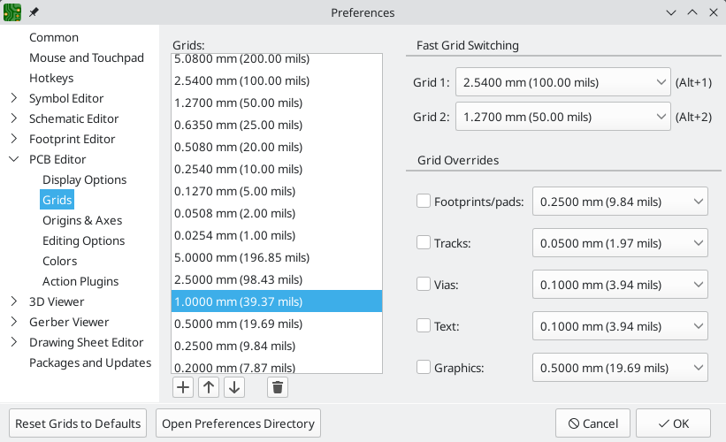
In this dialog you can select an active grid from the list of grids, reorder the list of grids, and add or remove grids. Grids defined in this dialog can have unequal X and Y spacing as well as an optional name.
This dialog also lets you designate two grids from the list as "Fast Grids", which can be quickly selected using Alt+1 and Alt+2.
Finally, you can configure grid overrides for different types of objects. Grid overrides let you set particular grid sizes for different types of objects which will be used instead of the default grid when working with those objects. For example, you can set a 100 mil grid for footprints and pads while using smaller grids to finely position tracks, vias, and text. Grid overrides can be individually enabled and disabled in this dialog, or globally enabled and disabled using the ![]() button on the left toolbar (Ctrl+Shift+G).
button on the left toolbar (Ctrl+Shift+G).
To change the origin (zero point) of the grid, use Place → Grid Origin and click to place the origin in the canvas. This function is also available with the ![]() button in the right toolbar. Alternatively, you can enter explicit coordinates for the grid origin with Edit → Grid Origin….
button in the right toolbar. Alternatively, you can enter explicit coordinates for the grid origin with Edit → Grid Origin….
The visual appearance of the grid can also be customized in several ways. You can change the thickness of the grid markings, switch their shape (dots, lines, or crosses), and set the minimum displayed spacing in the Display Options page of the preferences dialog, and you can change the grid color in the Colors page of the preferences dialog.
The grid can be shown or hidden using the ![]() button on the left-hand toolbar. By default the grid is still active even if it is hidden, but this is configurable in the Display Options preferences page. There you can set the grid to be disabled when it is hidden or even disable the grid entirely.
button on the left-hand toolbar. By default the grid is still active even if it is hidden, but this is configurable in the Display Options preferences page. There you can set the grid to be disabled when it is hidden or even disable the grid entirely.
编辑对象属性
All objects have properties that are editable in a dialog. Use the hotkey E or select Properties from the right-click context menu to edit the properties of selected item(s). You can only open the properties dialog if all the items you have selected are of the same type.
You can also view and edit item properties using the properties manager. The properties manager is a docked panel that displays the properties of the selected item or items for editing. If multiple types of items are selected at once, the properties panel displays only the properties shared by all of the selected item types.
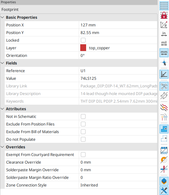
Editing a property in the properties manager immediately applies the change. When multiple items are selected, property modifications are applied to each selected item individually, not to the whole selection as a group. For example, when changing the orientation of multiple items, each item is individually rotated around its own origin, not the group’s origin.
Show the properties manager with View → Show Properties Manager or the ![]() button on the left toolbar.
button on the left toolbar.
Several tools are available for editing properties of specific types of objects in bulk. For text and graphical items, you can use the Edit Text and Graphics Properties tool. Tracks and vias can be bulk-edited using the Edit Track and Via Properties tool. Teardrop properties can be edited with the Edit Teardrops tool.
In properties dialogs and many other dialogs, any field that contains a numeric value can also accept a basic math expression that results in a numeric value.
For example, a dimension may be entered as 2 * 2mm, resulting in a value of 4mm. Basic arithmetic operators as well as parentheses for defining order of operations are supported.
电路板边框 (Edge Cuts)
KiCad 使用 Edge.Cuts 层上的图形对象来定义电路板的边框。 边框必须是一个连续(封闭)的形状,但可以由不同类型的图形对象组成,如直线和弧,或者是一个单一的对象,如矩形或多边形。 如果没有定义电路板的边框,或者电路板的边框无效,那么一些功能,如 3D 查看器和一些设计规则的检查将无法发挥作用。
使用封装
Adding footprints to the board
Footprints are automatically added to the board when the PCB is updated from the schematic. The footprint associated with each schematic symbol is added to the board if it is not already present, and each footprint pad is associated with the corresponding symbol pin’s net. Symbol pins are matched to footprint pads by pin/pad number.
When footprints are added to the board after an update from the schematic, they are grouped by schematic sheet and by geographical location in the schematic. They are initially attached to the cursor; you can place them by clicking in the desired location.
You can also add footprints to the board manually using the Add Footprint tool (A or the ![]() button).
button).
| Footprints added in this way will not be automatically associated with a symbol or have nets assigned to their pads, and subsequent updates from the schematic will remove these unassociated footprints unless the footprint is locked or the Delete footprints with no symbols option is unchecked in the Update PCB From Schematic dialog. For these reasons, it is usually recommended to avoid manually adding footprints to the board. Manually adding footprints is necessary for PCB-only workflows, and can also be useful for adding logos or other footprints that do not need a corresponding schematic symbol. |
Placing and moving footprints
Once footprints have been added to the board, you can reposition them in many ways.
The Move command (M) moves a footprint or a selection of footprints, ignoring any connected track segments that are not selected. No DRC checking is done when moving footprints with the Move command, although any footprint courtyards that collide with the moved footprint’s courtyard will be highlighted.
There is a reference point for the move operation, which is the point in the footprint which attaches to the cursor and therefore the point in the footprint that snaps to the grid and to other objects. The reference point during a move is determined by the location of the cursor when the Move command is initiated. If the cursor is over a pad, the pad’s center will be used as the reference point. If the cursor is not over a pad, the footprint’s anchor (coordinate origin point) will be used. To select an arbitrary snapping point, you can use the Move With Reference command instead of the regular Move command (right click → Positioning Tools → Move with Reference). After initiating the command, click on the desired reference point; KiCad will then begin the move with that point as the reference.
You can also use the Drag command (D) to move the selected footprint using the interactive router, maintaining all track connections to the footprint. Dragging footprints behaves like the Highlight Collisions router mode: obstacles will not be avoided or shoved, only highlighted. Ordinarily the router will prevent you from dragging a footprint into a position that violates DRC: when you click to commit a drag in a position that violates DRC, the footprint will return to its original position. To force a drag to be committed even if it violates DRC, Ctrl-click to commit the drag. Like the Move command, colliding courtyards are highlighted.
| Only tracks that end at the origin of the footprint’s pads will be dragged. Tracks that simply pass through the pad or that end on the pad at a location other than the origin will not be dragged. |
You can move a footprint to the opposite side of the board with the Flip command (F). Any parts of the footprint on a front layer will be swapped to the corresponding back layer, and vice versa.
Footprints can be rotated counter-clockwise using the R hotkey, or clockwise using Shift+R. By default, footprints are rotated by 90 degrees every time the rotate command is used, but you can configure the rotation angle step in Preferences → PCB Editor → Editing Options.
You can directly set a footprint’s exact absolute position, rotation angle, and PCB side using either the Footprint Properties dialog or the Properties panel.
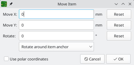
To reposition a footprint relative to its current position, use the Move Exactly tool (Shift+M). The dialog lets you specify an X and Y translation, as well as a rotation, that will be applied to the footprint. The rotation can be performed relative to either the footprint’s anchor, the local coordinate origin, or the drill/place origin. You can also use polar coordinates instead of Cartesian coordinates.
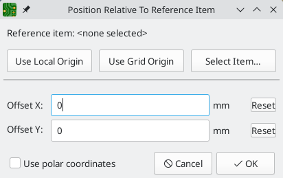
To position a footprint relative to another object, you can use the Position Relative tool (Shift+P). With this tool, you select a reference point for the move, which can be the local origin, the grid origin, or another arbitrary point, such as a pad in another footprint. The selected footprint is moved to the specified offset from the reference point.
You can swap the position of two selected footprints using the Swap command (S). The first footprint is assigned the location, rotation, and board side of the second footprint, and vice versa. If there are more than two footprints selected, the locations are cycled: the last footprint gets the position of the first footprint, the first footprint gets the location of the second, and so on.
There are several convenience features that make it easier to find, select, and move specific footprints or footprints related to another footprint.
The Get and Move Footprint command (T) prompts you to choose a footprint from a list or by typing a reference designator. KiCad then attaches the chosen footprint to your cursor for a move operation.
There are two commands to select other footprints that need to be connected to the selected footprint but don’t yet have routed connections. The Select All Unconnected Footprints command (O) selects all footprints that have ratsnest lines to the currently selected footprints. The command can be executed repeatedly to further expand the selection based on the newly selected items. The Grab Nearest Unconnected Footprint command (Shift+O) selects the closest footprint with ratsnest lines to the currently selected footprint, and additionally begins to move it. If there are multiple footprints initially selected, the command will act like the Move Individually command described below, individually moving the closest unconnected footprint for each of the initially selected footprints.
You can select footprints based on their schematic sheet using the right click → Select → Items in Same Hierarchical Sheet command, which selects all other footprints that are in the same schematic sheet as the originally selected footprint.
If you want to move multiple selected footprints in sequence, use the Move Individually command (Ctrl+M). After triggering the command, KiCad will begin moving the first selected footprint. After you click to place the footprint, KiCad will immediately start moving the next footprint, in the same order that you selected the footprints. You can skip moving a footprint by pressing Tab, commit the current move and skip any remaining moves by double-clicking, or cancel all moves (including those already completed) by pressing Esc.
If you want to move a collection of footprints at once into one area, the Pack and Move Footprints command (P) closely packs the selected footprints together and moves them as a block.
| Move Individually and Pack and Move Footprints are useful in combination with other selection convenience features, such as cross-selection from the schematic or the advanced footprint selection features described above. For example, you could select a group of bypass capacitors in the Schematic Editor, switch to the PCB Editor where the corresponding footprints are now selected, and then use Move Individually to quickly place all of the bypass capacitor footprints close to their respective ICs. Alternatively, you could use one of the other selection tools, such as Select All Unconnected Footprints, to select many footprints from all over the board, then use Pack and Move Footprints to quickly put them all into a small area. |
Finally, KiCad can automatically place footprints onto the board. The auto-place function attempts to optimally place footprints to simplify ratsnest connections to other footprints. You can auto-place the selected footprints with Place → Auto-Place Footprints → Place Selected Footprints, or auto-place all footprints outside of the board outline with Place → Auto-Place Footprints → Place Off-Board Footprints.
Editing Footprints
Footprints in the board can be individually edited. Editing a footprint in the board only affects that particular instance of the footprint; it does not affect any other copies of that footprint in the board, and it does not affect the library footprint.
To edit a footprint in the board, open its properties dialog (E)
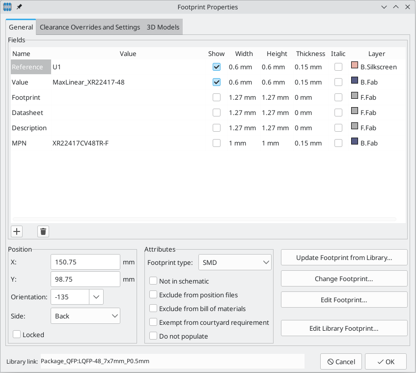
The majority of the settings in this dialog are the same as in the footprint editor. You can edit the footprint’s fields, attributes, clearance and zone connection settings, and 3D models, as in the footprint editor. However, here you can also set the footprint’s position, orientation, and side. You can also update the footprint from the library, exchange it for a different footprint, or edit the footprint itself in the footprint editor.
There are two options for editing the footprint in the footprint editor.
-
Edit Footprint… will open the specific instance of the footprint in the footprint editor. Editing this footprint will only affect this one instance of the footprint in the board. It will not affect other instances of the footprint in the board, and it will not affect the library copy of the footprint.
-
Edit Library Footprint… will open the library copy of the footprint in the footprint editor. Editing the library copy of the footprint will edit the footprint in the footprint library, but will not immediately affect any instances of that footprint in the board. To update footprints in the board with changes to the library footprint, use the Update Footprint from Library… tool.
Updating and exchanging footprints
When a footprint is added to the board, KiCad embeds a copy of the library footprint in the board so that the board is independent of the system libraries. Footprints that have been added to the board are not automatically updated when the library changes. Library footprint changes are manually synced to the board so that the board does not change unexpectedly.
To update footprints in the board to match the corresponding library footprint, use Tools → Update Footprints from Library…, or right click a footprint and select Update Footprint…. You can also access the tool from the footprint properties dialog.
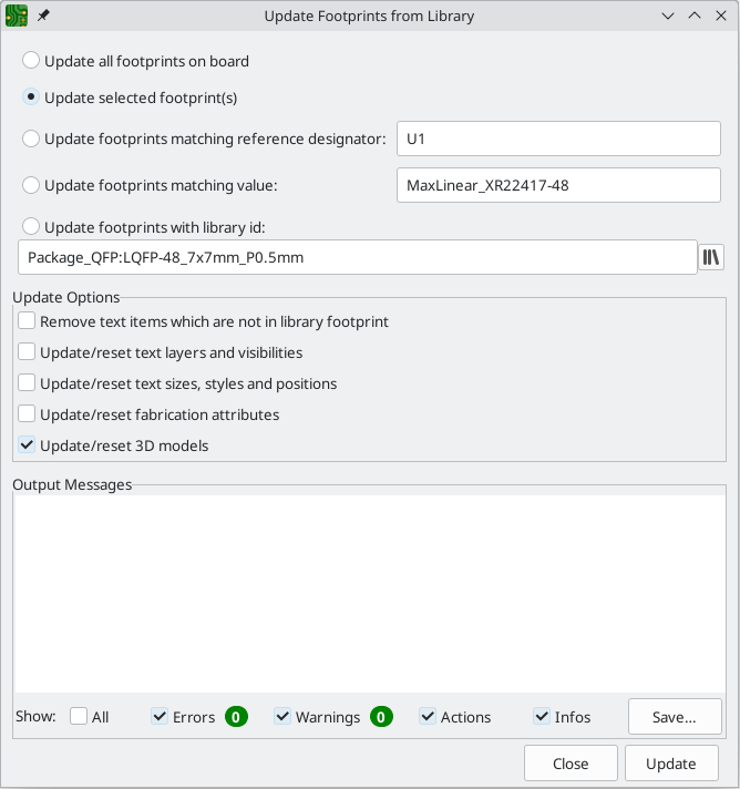
The top of the dialog has options to choose which footprints will be updated. You can update all footprints on the board, update only the selected footprints, or update only the footprints that match a specific reference designator, value, or library identifier. The reference designator and value fields support wildcards: * matches any number of any characters, including none, and ? matches any single character.
The middle of the dialog has options to control what parts of the footprint will be updated. You can select specific fields to update or not update, which properties of the fields to update (text, visibility, size and style, and position), and how to handle fields that are missing or empty in the library footprint. You can also choose whether to update footprint attributes, such as footprint type, not in schematic, exclude from position files / bill of materials, exempt from courtyard requirement, and do not populate.
The bottom of the dialog displays messages describing the update actions that have been performed.
To change an existing footprint to a different footprint, use Edit → Change Footprints…, or right click an existing footprint and select Change Footprint…. This dialog is also accessible from the footprint properties dialog.
The options for the Change Footprints dialog are very similar to the Update Footprints from Library dialog.
Editing footprint fields
An individual symbol text field can be edited directly with the E hotkey (with a field selected instead of a footprint) or by double-clicking on the field.
The options in this dialog are the same as those in the full Footprint Properties dialog, but are specific to a single field.
Only footprint fields can be edited this way in the board editor. Unlike fields, Footprint text is a graphic object that can only be edited or moved in the footprint editor.
| In versions of KiCad before version 8.0, footprint fields did not exist. Instead, footprint text could be edited directly in the board editor. In KiCad 8.0, footprint text is not editable in the board editor and can only be edited in the footprint editor. |
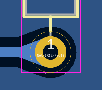
使用焊盘
在将封装放置在电路板上之后,可以检查和编辑封装的每个单独的焊盘的属性。 换句话说,如果库中的封装设计不合适,就可以在电路板上封装的特定实例中覆盖单个封装焊盘的设计。 例如,你可能希望为一个需要在特定设计中保持不焊接的焊盘去除锡膏孔,或者你可能希望移动一个轴向引线电阻的通孔焊盘的位置,以适应特定的设计。
| 默认情况下,所有封装焊盘的位置都被锁定,因此可以编辑焊盘属性,但不能移动焊盘相对于封装其他部分的位置。 焊盘可以被解锁以允许自由移动,这对某些应用很有用(如具有不同引线位置的通孔封装),但通常不建议用于表面贴装封装。 |
当一个焊盘被选中时,焊盘属性对话框将通过上下文菜单或默认的快捷键 E 打开。 请注意,KiCad 认为如果你在焊盘附近点击,你可能是想选择整个封装而不是单个焊盘。 要选择单个焊盘,请确保在焊盘区域内点击,或者关闭选择过滤器中的 "封装" 设置(并确保 "焊盘" 设置打开),以防止意外地选择整个封装而不是特定的焊盘。
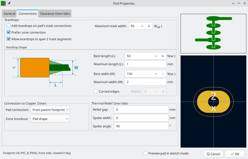
This dialog lets you edit the physical properties of the pad, including size and shape. You can also modify how the pad connects to other objects on the board, including clearance properties, teardrops, and thermal reliefs.
This dialog is the same as the pad properties dialog in the footprint editor, except that here you can also manually assign a net to a pad using the net name selector. The remaining options are explained in the Footprint Editor documentation.
| While you can manually assign nets to pads in the PCB editor, this is not a typical workflow. Usually net-to-pad connections are defined by the schematic and then transferred to the PCB editor. |
使用敷铜
敷铜区域,有时也被其他 EDA 工具称为铺铜或覆铜,是分配给一个特定网络的实心或网格状的铜箔区域,敷铜区域会自动保持与其他铜对象的间隙。 敷铜区域通常用于填充板层(或板层的一部分)上的所有自由空间,以创建接地和电源平面,承载大电流,或提供屏蔽。
| 一些 EDA 工具有单独的工具用于创建 "平面层" 及在信号层上创建敷铜区域。 在 KiCad 中,敷铜工具用于这两种应用。 |
区域是由一个多边形的 边框 来定义的,它定义了敷铜区域的最大范围。 这个边框并不代表实物铜,也不会出现在导出的制造数据中。 每次修改边框或边框内的任何对象时,必须 填充 该敷铜区域。 填充过程可以在单个敷铜区域上运行,也可以在电路板的所有区域上运行(默认快捷键 B)。 敷铜区域可以 不填充(默认快捷键 Ctrl+B),以提高性能并减少编辑大型电路板时的视觉混乱。
| By default, zone filling is a manual process rather than occurring every time an object changes that would result in a change to the zone copper. This is because zone filling can be a slow process on older computers or very large designs. It is important to make sure zone fills are up-to-date before generating outputs. KiCad will check that zones have been updated and warn you before generating outputs or running DRC when zones have not yet been refilled. You can optionally enable automatic zone-filling in the Preferences dialog (PCB Editor → Editing Options → Miscellaneous → Automatically refill zones). |
要绘制一个敷铜区域,请点击右侧工具栏的 “添加敷铜区域” 工具(![]() ),或者使用默认的快捷键 Ctrl+Shift+Z。 点击选择敷铜区域边框的第一个点。 敷铜区域属性对话框将出现,允许你选择敷铜区域的网络和其他属性。 这些属性可以在任何时候进行编辑,所以一开始正确选择它们并不是关键。 接受该对话框,继续放置点来定义敷铜区域的边框。 要完成这个区域,请双击来设置最后一个点。敷铜区域边框点可以像图形多边形一样进行修改,通过拖动方形手柄来移动一个角,或者拖动圆形手柄来移动一条边。 要编辑该敷铜区域的属性,请使用快捷键 E 或从上下文菜单中选择 “属性”。
),或者使用默认的快捷键 Ctrl+Shift+Z。 点击选择敷铜区域边框的第一个点。 敷铜区域属性对话框将出现,允许你选择敷铜区域的网络和其他属性。 这些属性可以在任何时候进行编辑,所以一开始正确选择它们并不是关键。 接受该对话框,继续放置点来定义敷铜区域的边框。 要完成这个区域,请双击来设置最后一个点。敷铜区域边框点可以像图形多边形一样进行修改,通过拖动方形手柄来移动一个角,或者拖动圆形手柄来移动一条边。 要编辑该敷铜区域的属性,请使用快捷键 E 或从上下文菜单中选择 “属性”。
层: 一个区域对象可以在一个或多个铜层上创建敷铜。 勾选每个铜层旁边的方框,就会在选中层的区域边框内进行敷铜。 每个层上的铜将被独立地填充,但所有层将共享同一个网络。
网络: 选择该敷铜区域应连接的电气网络。 可以创建没有网络分配的区域。 没有网络的区域将与任何网络上的任何铜对象保持间隙。
区域名 可以用来给一个区域指定一个特定的名称。 这个名字可以用来在自定义的 DRC 规则中指代该区域。
Zone priority level determines the order in which multiple zones on a single layer are filled. The highest priority level zone on a given layer will be filled first. Lower-priority zones will keep clearance to the filled areas of higher-priority zones. Two zones on the same layer with the same priority level will overlap (short-circuit) with each other, unless they are assigned different nets. When two zone outlines with the same priority and different nets touch, one zone will maintain clearance to the other so that they don’t short.
锁定 控制敷铜区域边框对象是否被锁定。 被锁定的对象不能被操作或移动,也不能被选择,除非在选择过滤器面板中启用 锁定项目 选项。
边框显示 控制敷铜区域边框在屏幕上的绘制方式。 在 直线 模式下,只绘制边框的边界线。 在 阴影 模式下,阴影线会在边框边界的内侧绘制一小段距离,以使敷铜区域边框更加明显。 在 完全阴影 模式下,阴影线被绘制在整个区域边框的内部。
Corner smoothing controls the behavior of the filled copper areas at corners of the outline. Corners can be smoothed by a chamfer or fillet, or can extend all the way to the outline corner if smoothing is disabled. The chamfer or fillet size is configurable when those modes are selected.
| 默认情况下,倒角和圆角不会被添加到区域边框的内角,因为这将导致填充的铜延伸到边框之外。 如果需要光滑的内角,请在电路板设置对话框的约束部分启用 允许敷铜区域边框外的圆角 选项。 |
间隙 控制该敷铜区域与其他铜对象保持的最小间隙。 请注意,如果两个间隙值有冲突,将使用较大的间隙值。 例如,如果一个敷铜区域被设置为使用 0.2 毫米的间隙,但其网络类被设置为使用 0.3 毫米的间隙,结果将是 0.3 毫米的间隙。
最小宽度 控制在该敷铜区域内产生的铜窄颈(narrow neck)的最小尺寸。 任何低于这个最小宽度的敷铜区域都会在填充过程中被移除。
焊盘连接 控制敷铜区与同一网络上的封装焊盘的连接方式。 实心 连接将使得铜完全重叠在焊盘上。热焊盘 将导致小铜辐条连接焊盘和敷铜区域的其余部分,增加焊盘和敷铜区域的其余部分之间的热阻。 这对手工焊接很有用。 对 PTH 的热焊盘 将对电镀通孔焊盘应用热焊盘,并对表面贴装焊盘使用实心连接。 无 将导致该敷铜区域不连接到同一网络上的任何焊盘。
热焊盘间隙 控制任何焊盘和敷铜区域之间保持的距离(当焊盘连接模式被设置为热焊盘时)。
热焊盘辐条宽度 控制 "辐条" 的宽度,即连接焊盘和其他敷铜区域的短铜段。
填充类型 控制敷铜区域的填充方式:默认为 实心填充,这将使得敷铜填充到区域边框内的所有可用空间。 敷铜区域也可以被设置为 网格填充,这将使该区域充满网格状的敷铜(铜较少)。 这对于柔性印刷电路和其他专业应用非常有用。
方向 控制网格模式中线的角度。 0 度方向将使网格使用水平和垂直的线条。
网格宽度 控制网格模式中每条线的宽度。
网格间隙 控制网格模式中每条线之间的距离。
平滑效果 控制应用于网格模式的平滑风格。值为 0 为无平滑,值为 3 为最精细的平滑。 值越大将导致更长的处理时间和更大的 Gerber 文件。
平滑量是一个比率, 控制当 平滑效果 设置为 0 以外的值时生成的平滑倒角或圆角的大小。值为 0.0 表示没有平滑,值为 1.0 表示最大平滑(换句话说 ,倒角或圆角等于网格间隙的一半)。
移除死铜 控制孤立铜区域(也称为孤岛)在初始敷铜后行为。 当设置为 总是 时,敷铜区域内的孤立铜会被移除。当设置为 从不 时,孤立区域会被搁置,并会导致该敷铜区域不与任何其他网络连接。 当设置为 低于敷铜限制 时,可以指定一个 最小的孤岛尺寸,低于这个阈值的孤岛将被删除。
| 无论 移除死铜 设置如何,死铜都不会从没有电气连接的敷铜区域中移除。 换句话说,仅可以从具有至少一个电气连接的敷铜中移除死铜。 |
布线
KiCad 具有交互式布线器的功能:
-
Allows manual or guided (semi-automatic) routing of single tracks and differential pairs
-
可通过以下方式修改现有设计:
-
拖动已有导线时进行重新布线
-
拖动封装时对连接到封装焊盘的导线进行重新布线
-
-
允许通过插入蛇形线
+来调整布线长度和差分对的偏移(相位) 为具有严格时序要求的设计调整布线形状
默认情况下,布线器在放置布线时遵循配置的设计规则:新布线的尺寸(宽度)将取自设计规则。在确定新布线和过孔的放置位置时,布线器将遵循设计规则中设置的铜间隙。 如果需要的话,可以通过使用高亮冲突布线器模式,或打开布线器设置中的 “允许 DRC 违规” 选项来禁用这种行为(见下文)。
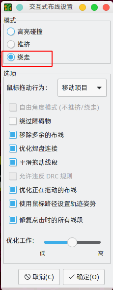
布线器有三种模式,可以随时选择。 布线器的模式用于新的布线,但也用于使用拖动(快捷键 D)命令拖动现有布线。 这些模式是:
-
高亮碰撞:在此模式下,大部分布线器功能被禁用,布线完全手动。 布线时,碰撞 (间隙违规) 将以绿色高亮,如果存在冲突,则新的布线无法在该位置放置,除非打开了 “允许 DRC 冲突” 选项。 在此模式下,一次最多可以放置两个布线段 (例如,一个水平线段和一个斜线段)。
-
推挤:在此模式下,布线的线段将绕过无法移动的障碍物 (例如,焊盘和锁定的布线/过孔)并 推挤 可以移动的障碍物。布线器在此模式下会防止违反 DRC:如果在不违反 DRC 的前提下,光标位置无法进行布线,则不会创建新的布线。
-
绕走:在此模式下,布线器的行为与推挤模式相同,只是不会移动障碍物。
使用哪种模式是一个偏好问题。 对于大多数用户,我们建议使用推挤模式以获得最高效的布线体验。如果您不希望布线器修改未被布线的线段,则建议使用绕走模式。请注意,推挤和绕走模式始终创建水平、垂直和 45 度 (H/V/45) 布线段。如果需要使用 H/V/45 以外的角度布线段,则必须使用高亮碰撞模式,并在交互布线器设置对话框中启用自由角度模式选项。
There are four main routing functions: Route Single Track, Route Differential Pair, Tune length of a single track, and Tune skew of a differential pair. All of these are present in both the Route menu dropdown (individually) on the top toolbar and the drawing toolbar in two overloaded icons on the drawing toolbar on the right. The use of the overloaded icons is described above. One is for the two Route functions and one is for the two Tune functions. In addition, the Route menu allows the selection of Set Layer Pair and Interactive Router Settings.
要进行布线布线,请点击布线 ![]() 图标(从绘图工具栏或从顶部工具栏 布线 菜单中)或使用快捷键 X。 点击一个起始位置,选择要布线的网络,并开始布线。 布线的网络会自动高亮显示,网络允许的间隙会在当前布线的周围用灰色的轮廓表示。 可以通过改变 "偏好设置" 对话框中的 "间隙轮廓" 设置来禁用间隙轮廓功能。
图标(从绘图工具栏或从顶部工具栏 布线 菜单中)或使用快捷键 X。 点击一个起始位置,选择要布线的网络,并开始布线。 布线的网络会自动高亮显示,网络允许的间隙会在当前布线的周围用灰色的轮廓表示。 可以通过改变 "偏好设置" 对话框中的 "间隙轮廓" 设置来禁用间隙轮廓功能。
| 间隙轮廓显示从布线网络到 PCB 上任何其他铜对象的最大间隙。 可以使用自定义设计规则为不同对象指定网络的不同间隙。 布线器将考虑这些间隙,但仅直观地显示最大间隙值。 |
当布线器处于活动状态时,将从布线起点到编辑器光标绘制新的线段。这些线段是未固定的临时 (unfixed temporary) 对象,它们显示当您左键鼠标或 Enter 键来确定布线 (fix the route) 时将创建哪些线段。非固定布线段以比固定布线段更亮的颜色显示。当您使用 Esc 键或通过选择另一个工具退出布线器时,将只保存固定布线段。完成布线操作(快捷键 End) 将固定所有布线并退出布线器。
在布线时,可以使用 "撤消上一个布线段" 命令 (快捷键 Backspace) 取消上一个固定的布线。您可以重复使用此命令后退已固定的布线。
In previous versions of KiCad, using the left mouse button or Enter to fix the routed segments would fix all segments up to but not including the segment ending at the mouse cursor location. In KiCad 6 and later, this behavior is optional, and by default, all segments including the one ending at the mouse cursor location will be fixed. The old behavior can be restored by disabling the "Fix all segments on click" option in the Interactive Router Settings dialog.
布线时,可以按住 Ctrl 键禁用网格捕捉,按住 Shift 键禁用对焊盘和过孔等对象的捕捉。
| 也可以通过更改偏好设置对话框的编辑选项部分中的磁吸点首选项来禁用对象的捕捉。 我们建议您在一般情况下保持启用对象捕捉,这样就不会意外地在焊盘或过孔上略微偏离中心结束布线。 |
布线形态
在水平(H) / 垂直 (V) / 45 度模式下布线时,形态 是指一组两个线段如何连接单个 H/V/45 度线段无法到达的两个点。 在这种情况下,这些点将由一条水平或垂直线段和一条斜线段 (45度) 连接。形态指的是这些线段的顺序:是水平/垂直线段在前还是斜线段在前。


KiCad 的布线器会尝试根据一系列因素自动选择最佳形态。一般说来,布线器会尝试最大限度地减少路线中的拐角数量,并尽可能避免 "槽糕" 的拐角 (如锐角)。当从焊盘布线或布线到焊盘时,KiCad 将选择使路线与焊盘最长边缘对齐的形态。
在某些情况下,KiCad 无法正确猜测您想要的形态。要在布线时切换布线的形态,请使用切换布线形态命令 (快捷键 /)。
在没有明显的 “最佳” 形态的情况下(例如,从过孔开始布线时),KiCad 将使用鼠标光标的移动来选择形态。如果希望布线从直线 (水平或垂直) 线段开始,请在水平或垂直方向上将鼠标从起始位置移开。如果您希望布线以斜线开始,请沿斜线方向移动。一旦光标与布线起始位置相距足够远,形态就会被锁定,并且除非光标回到起始位置,否则不会再更改。可以在交互式布线器设置对话框中禁用从鼠标光标移动检测形态,如下所述。
| 如果使用切换布线形态(Switch Track Posture)命令覆盖 KiCad 选择的形态,则在当前布线操作的剩余部分中,将禁用鼠标移动姿势的自动检测。 |
布线转角模式
当以 H/V/45 模式布线时,KiCad 的布线器可以放置尖角或圆角 (弧形) 的布线。要在尖角和圆角之间切换,请使用布线拐角模式命令 (快捷键 Ctrl+/)。使用圆角布线时,每个布线步骤将放置直线段、单个圆弧或同时放置直线段和圆弧。布线形态决定首先放置圆弧还是直线段。
Track corners can also be rounded after routing by using the Fillet Tracks command after selecting the tracks on either side of the corner to be filleted. If a contiguous track selection contains multiple corners, they will all be filleted.
| Dragging of tracks with arcs is not supported. Arcs are treated as immovable by the shove router. |
布线宽度
布线的线段的宽度是通过以下三种方式之一来确定的:如果布线的起点是现有线段的终点,并且顶部工具栏上的 ![]() 按钮被启用,宽度将被设置为现有布线的宽度。 否则,如果顶部工具栏中的布线宽度下拉菜单被设置为 "使用网络类宽度",则宽度将取自布线的网络类(或任何为网络类指定不同宽度的自定义设计规则,例如在颈缩区域内)。 最后,如果布线宽度下拉菜单被设置为电路板设置对话框中配置的预定义布线尺寸之一,则将使用该宽度。
按钮被启用,宽度将被设置为现有布线的宽度。 否则,如果顶部工具栏中的布线宽度下拉菜单被设置为 "使用网络类宽度",则宽度将取自布线的网络类(或任何为网络类指定不同宽度的自定义设计规则,例如在颈缩区域内)。 最后,如果布线宽度下拉菜单被设置为电路板设置对话框中配置的预定义布线尺寸之一,则将使用该宽度。
| 布线宽度永远不能小于在电路板设置对话框的约束部分中配置的最小布线宽度。如果添加的预定义宽度低于此最小约束,则将使用最小约束值。 |
KiCad 的布线器支持活动布线过程中的布线宽度调整。 换句话说,要改变导线中间的宽度,必须结束布线,然后从上一个布线的末端重新开始一条新的布线。 要改变活动布线的宽度,可使用快捷键 W 和 Shift+W,切换在电路板设置对话框中配置的布线宽度。
放置过孔
在进行布线时,切换层会在当前(未固定)导线的末端插入一个过孔。 一旦你放置了过孔,布线将继续在新层上进行。 有几种方法可以选择一个新层并插入过孔:
-
使用快捷键选择特定的图层,如 PgUp 选择
F.Cu或 PgDn 选择B.Cu。 -
通过使用 "下一层" 或 "上一层" 快捷键 (+ 和 -)。
-
通过使用 "放置过孔" 快捷键 (V),切换到活动层对中的下一层。
-
通过使用 "选择图层并放置通孔过孔" 操作(快捷键 <),将打开一个对话框来选择目标层。
After using any of the above methods to add a via and change layer, but before clicking to fix the via and commit the current trace segment, you can cancel placing the via by pressing V. The via will be removed and routing will continue on the original layer.
You can place a via and end the current trace, without changing layers, by pressing V and then double-clicking or Shift-clicking to place the via.
过孔的尺寸将取自当前的 “过孔尺寸” 设置中,可通过顶部工具栏的下拉列表或使用快捷键 (') “增加过孔尺寸” 及快捷键 (\) “减小过孔尺寸” 。与布线宽度类似,当过孔大小设置为"使用网络类尺寸" 时,将使用 "电路板设置" 的 "网络类" 部分中配置的过孔大小 (除非被自定义设计规则覆盖)。
You can also place microvias and blind/buried vias while routing. Use the hotkey Ctrl+V to place a microvia and Alt+Shift+V to place a blind/buried via. Microvias may only be placed such that they connect one of the outer copper layers to an adjacent layer. Blind/buried vias may be placed on any layer.
布线器放置的过孔被认为是已布线导线的一部分。 这意味着过孔网络可以自动更新(就像导线网络一样),例如,当从原理图中更新 PCB 时改变了导线的网络名。 在某些情况下,这可能是不需要的,例如在创建缝合孔时。 对于特定的过孔,可以通过关闭过孔属性对话框中的 "自动更新过孔网络" 复选框来禁用过孔网络的自动更新。 使用 "添加独立过孔" 工具放置的过孔在创建时禁用这一设置。
Routing Convenience Functions
KiCad offers several functions to make certain routing operations more convenient.
If you need to route a number of traces from a set of pads, you can use the Route Selected tool to quickly route from each pad in sequence. Select the pads you want to use as starting points, then press Shift+X to route from each pad in sequence. The router will begin a trace from the first selected pad, which you can route as you would any other trace. When you complete the trace, the router will automatically begin a new trace from the next pad in the selection, in the same order that you selected the pads. Pads that already have traces attached are skipped. You can also skip routing the current trace and move on to the next pad by pressing Esc. You can also select footprints instead of pads; all unrouted pads in the selected footprints will be used as starting points.
If you want to route a number of traces to a set of pads, instead of from the pads, you can use the Route Selected From Other End tool (Shift+E). This tool works the same way as the Route Selected tool, except it uses each selected pad as an end point rather than a starting point. The starting point for each trace is the other end of the ratsnest line for each selected pad.
Routing from the other end is also possible while routing individual traces: press Ctrl+E while routing a trace to commit the current segment and begin routing from the other end of the in-progress trace’s ratsnest line.
Finally, you can quickly unroute traces connected to an object (footprint, pad, or trace) by selecting the object, right-clicking, and selecting Unroute Selected. Any traces connected to the selected object will be removed, starting at the selected object and continuing until another pad is encountered.
Automatically completing traces
KiCad’s router can automatically route individual traces, based on the connections defined in the schematic. This can be thought of as a limited form of auto-routing that considers a single trace at a time. The router will only use the current layer; it will not use vias or change layers.
While routing, press the F key to have the router attempt to automatically finish the current trace. The trace will be automatically routed from the end of the last fixed trace segment to the closest ratsnest anchor. If the router can’t automatically finish the trace, it will allow you to complete the trace manually. This action can also be performed by clicking Attempt Finish in the context menu while routing.
When the router is not the active tool, you can automatically route multiple traces by selecting footprints, pads, and traces to route from and pressing Shift+F. You do not need to select both ends of a desired connection; the router will route from the selected item to its nearest ratsnest anchor. If multiple items were selected, each item will be routed in sequence, in the order that they were selected. If a connection cannot be automatically completed, the tool will pause with the router active so that you can complete the trace manually. With the automatic completion paused for a manual connection, you can press Esc to skip routing the current trace. After manually completing the trace or skipping the connection, the tool will continue attempting to route the remaining connections.
差分对布线
Differential pairs in KiCad are defined as nets with a common base name and a positive and negative suffix. KiCad supports using + and -, or P and N as the suffix. For example, the nets USB+ and USB- form a differential pair, as do the nets USB_P and USB_N. In the first example, the base name is USB, and USB_ in the second. The suffix styles cannot be mixed: the nets USB+ and USB_N do not form a differential pair. Make sure you name your differential pair nets accordingly in the schematic in order to allow use of the differential pair router in the PCB editor.
要对差分对进行布线,请点击差分对布线 ![]() 图标(从绘图工具栏或从顶部工具栏 布线 下)或使用快捷键 6。 点击一个焊盘、过孔或现有差分对线段的末端,开始布线。 你可以从差分对的正网络或负网络开始布线。
图标(从绘图工具栏或从顶部工具栏 布线 下)或使用快捷键 6。 点击一个焊盘、过孔或现有差分对线段的末端,开始布线。 你可以从差分对的正网络或负网络开始布线。
差分对布线器将尝试用设计规则中的间隙规则进行布线(差分对间隙可以在电路板设置对话框的 “网络类” 部分中配置,也可以通过使用自定义设计规则来配置)。如果布线的起始或结束位置与配置的间隙不同,布线器将创建一个较短的 "扇出" 部分,以最大限度地缩短差分对未耦合的布线长度。
当切换层或使用 放置过孔 (V) 操作时,差分对布线器将创建两个相邻的过孔。这些过孔将被放置在尽可能靠近彼此的位置,同时遵守铜的间隙规则以及孔到孔的间隙规则。
修改布线
布线完成后,可以通过移动或拖动来修改它们,或者删除并重新布线。 当选择一个导线时,快捷键 U 可以用来将选择范围扩大到所有连接的导线。 第一次按下 U 将选择与焊盘或过孔最近的连接点之间的导线。 第二次按 U 将再次扩大选择范围,包括所有层上与所选导线相连的所有导线。 用这种技术选择导线可以用来快速删除整个布线网络。
有两种不同的拖动命令可用于修改导线。拖动 (45 度模式) 命令,快捷键 D ,用于通过布线器拖动导线。如果布线器模式设置为推挤,则使用此命令拖动将推挤附近的布线。如果布线器模式设置为绕走,则使用此命令拖动将绕过障碍物或停在障碍物处。以自由角度拖动命令,快捷键 G,用于将导线一分为二,并将新的角拖动到任何位置。以自由角度拖动的行为类似于高亮碰撞布线器模式:不会避开或推挤障碍物,只会高亮。
| 目前还不能拖动包含圆弧的布线。在某些情况下,尝试拖动这些布线会导致圆弧被删除。可以通过选中特定圆弧并使用拖动命令 (D) 来调整其大小。使用此命令调整圆弧大小时,不执行 DRC 检查。 |
移动命令(快捷键 M)也可以在导线上使用。 该命令将拾取选定的导线,而忽略任何未被选中的附加导线或过孔。 使用移动命令移动导线时,不会进行 DRC 检查。
在移动封装的同时,可以对连接在封装上的导线进行重新布线。 要做到这一点,在选择了一个封装的情况下使用拖动命令(D)。 任何以封装的某个焊盘为终点的导线都将与封装一起被拖动。 这个功能有一些限制:它只在高亮冲突模式下运行,所以连接在封装上的导线不会绕过障碍物或将附近的导线推开。 此外,只有以封装的焊盘为终点的导线才会被拖动。 仅仅经过焊盘或在焊盘原点以外的焊盘上结束的导线将不会被拖动。
You can modify the width of tracks and the size of vias, without re-routing them, in the properties of the track or via. You can choose a predefined size or set the size to an arbitrary value. You can also change the position of tracks and vias or change a via’s start and end layers.
To modify tracks and vias in bulk you can use the Edit Track and Via Properties dialog (Edit → Edit Track & Via Properties…)..
Scope settings restrict the tool to editing only tracks, vias, or both. If no scopes are selected, nothing will be edited.
Filter Items restricts the tool to editing particular objects in the selected scope.
Objects will only be modified if they match all enabled and relevant filters
(some filters do not apply to certain types of objects. For example, via size
filters do not apply to tracks). If no filters are enabled, all objects in the
selected scope will be modified. For filters with a text box, wildcards are
supported: * matches any characters, and ? matches any single character.
Filter items by net filters to items assigned the specified net. Filter items by netclass filters to items assigned to the specified netclass.
按层筛选对象 筛选到指定板层上的对象。
Filter tracks by width filters to tracks with the specified track width. Filter vias by size filters to vias with the specified track width.
Selected items only filters to the current selection.
Properties for filtered objects can be set to new values in the bottom part of the dialog. Properties can be set to arbitrary values by selecting set to specified values or set to the default value from the net class (or custom rule) by selecting set to net class / custom rule values.
Drop-down lists can be set to -- leave unchanged -- to preserve existing values, or set to a pre-defined track or via size to change the filtered objects' size. You can also change the filtered objects' layer.
长度调整
The length tuning tools can be used to add serpentine tuning shapes to tracks after routing. Length tuning shapes are persistent objects that can be modified after they are created. To tune the length of a track, first pick the appropriate tool.
-
The single-track length tuning tool (icon
 or hotkey 7) will add serpentine shapes to bring the length of a single track up to the target value.
 -
The differential pair length tuning tool (icon
 or hotkey 8) will do the same for a differential pair.
 -
The differential pair skew tuning tool (icon
 or hotkey 9) will add length to the shorter member of a differential pair in order to eliminate skew (phase difference) between the positive and negative sides of the pair.
As with the Routing icons, the Tuning icons are found in both the Route menu dropdown from the top toolbar and the drawing toolbar on the right.
When a tuning tool is active, you can hover over traces in the board to show a status window that displays their current length or skew as well as the target values. Click on the desired trace to start tuning it. As you move the mouse cursor along the track, meander shapes will be added interactively. If a target length has been set, meanders will stop being added when the target length is reached. You can set a target length with custom DRC rules or in the tuning shape properties; both methods are explained below. The popup window next to the cursor shows a live measure of the length or skew compared to the design targets. You can adjust the spacing (1 to increase and 2 to decrease) and amplitude (3 to increase and 4 to decrease) while you tune. When you are done, click again to commit the tuned shape. The tuned trace doesn’t need to be perfect because you can adjust the shape after committing it. You can also place multiple tuning shapes on the same track.
| The length tuning tools only support tuning the length of point-to-point nets between two pads. Tuning the length of nets with different topologies is not supported. |
| Differential pair length tuning can only be applied to the coupled portions of differential pairs. To apply length tuning to the uncoupled portions of differential pairs, you must use single-track length tuner. |
Editing tuning patterns
After a tuning pattern has been added, it can be selected, modified, and moved. While it is selected, the target length and routed length are shown in the message panel at the bottom left of the window.
When a pattern is selected, editing handles appear, which let you adjust the pattern geometry.
-
Dragging the handles at the ends of the pattern will expand or contract the pattern along the trace.
-
Dragging the corner handle towards or away from the trace will respectively decrease or increase the maximum meander amplitude.
-
The final handle controls the meander spacing; dragging it towards the corner handle will increase the spacing, while dragging it away from the corner handle will increase the spacing.
The selection box and editing handles represent the maximum allowable extents of the tuning pattern. Making the box smaller will reduce the size of the tuning pattern, even if this results in the tuned trace being shorter than the target length. When the box is enlarged, the tuning pattern will expand to fill the box until the target length is reached.
You can move a tuning pattern along its track by selecting it and dragging with the mouse, or using the Move tool (M). Deleting a tuning pattern (Del) removes the tuning pattern and restores the original untuned tracks. You can also ungroup the tuning pattern, which will decompose it into its component tracks. The basic tracks have the same shape as the tuning pattern but can be edited individually. Once ungrouped into tracks, a tuning pattern cannot be regrouped.
Another way to edit a tuning pattern is through its properties dialog. The properties dialog exposes several additional parameters that can’t be modified using the on-canvas interactive editor. These properties can also be edited in the properties manager.
As with the interactive editor, you can set a maximum amplitude for the tuning pattern and a spacing between meanders, but here you can set a minimum amplitude and configure the corner style. Corners can be filleted (rounded) or chamfered. In each case you can set the radius as a percentage of the maximum possible radius for the spacing and amplitude. You can also configure the tuning pattern to be single-sided, which restricts it to one side of the baseline, as opposed to the default style which positions meanders on both sides of the baseline.
You can set default values for these properties in the Design Rules → Length-tuning Patterns page of the Board Setup dialog. Each type of tuning pattern (single track length, differential pair length, and differential pair skew) can have its own defaults.
Finally, the tuning pattern properties dialog is one of two ways to set the target length or skew for a tuning pattern. Setting length targets is explained below.
Setting target length and skew
There are two ways to set a target length or skew for a net:
-
In the properties dialog for a tuning pattern that has already been added to a track.
-
Using a custom DRC rule with the
lengthand/orskewconstraints.
The first method is to specify a target in the target length or target skew field of the tuning pattern’s properties dialog. This target will only apply to the selected tuning pattern. Therefore, length targets set in this way must be set separately for each tuning pattern in the design. The properties dialog for a tuning pattern is only accessible after the pattern is initially created, so changing a target length or skew in this way may require the pattern to be adjusted to meet the new target value, if the pattern’s geometric constraints do not allow sufficient space to meet the new target.
You can also set a target length and/or skew using custom design rules. If custom rules are used, they will override any targets set in tuning pattern properties, unless the override custom rules checkbox is enabled in the tuning pattern properties.
Using a custom rule allows you to set a net’s target length and/or skew up front, before a pattern is created. With custom rules you can set different length and skew targets based on specific criteria, such as netclass or net name. You will also result in a DRC violation if the net’s length or skew is out of bounds.
When target length or skew is adjusted in a custom DRC rule after a pattern is created, the pattern geometry will not be automatically updated to achieve the new target. You can use Edit → Update All Tuning Patterns to recalculate all tuning patterns to meet the new targets.
The following example custom rule sets a target length and skew for nets in the high_speed netclass. The target length is 100mm, and a DRC error will be raised if it is below 95mm or above 105mm. The target skew is at most 0.1mm.
(rule "target length and skew"
      (condition "A.NetClass == 'high_speed'")
      (constraint length (min 95mm) (opt 100mm) (max 105mm))
      (constraint skew (max 0.1mm)))
See the custom rule documentation for more details of how to create rules that only apply to certain nets.
Length tuning pitfalls and tips
The length tuner only tunes nets with a point-to-point topology; branching nets are not supported. When the length tuner encounters a branch, it stops at the branch and only considers the length of the net up to that branch.
Sometimes you may end up with leftover stub tracks somewhere in your design. These can turn what appears to be a point-to-point net into a branched topology, which will prevent length tuning from working as expected. It may be easier to find such stub tracks when you switch footprints, vias, and tracks to outline mode (![]() ,
, ![]() , and
, and ![]() buttons, respectively). You can also use the track cleanup tool (Tools → Cleanup Tracks and Vias…) to remove many of these stubs automatically.
buttons, respectively). You can also use the track cleanup tool (Tools → Cleanup Tracks and Vias…) to remove many of these stubs automatically.
By default, the length tuner includes vias in its length calculations. Only the layer-to-layer length of the via is used, which may be shorter than the full top-to-bottom via height if the tuned path is not exclusively on the board top and bottom. The accuracy of this calculation depends on the board stackup being accurately configured. Via length can be ignored in length tuner calculations by deselecting include stackup height in track length calculations in the Constraints page of the Board Setup dialog.
The length tuner is optimized for adjusting the effective electrical distance between two points, and therefore it calculates net length in a slightly different way than other tools, such as the Net Inspector. In addition to discounting net branches and unused portions of vias, the length tuner also optimizes paths through pads to use the shortest possible path in its calculations. In comparison, the Net Inspector reports a simple summation of copper segment lengths. Both calculations are accurate, but they are optimized for different purposes. These differences are discussed in more detail in the Net Inspector documentation.
Teardrops
Teardrops are areas of extra copper that smooth the transition between track and pads, vias, or other tracks. Teardrops are added to increase the mechanical robustness of a trace connection. They also reduce the risk of a misaligned drill hole disconnecting a trace from a drilled pad or via.
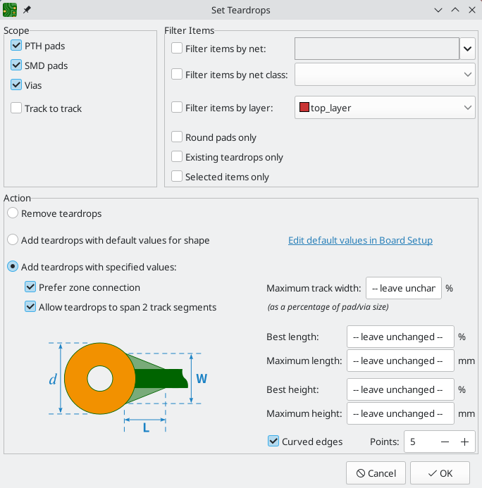
You can add teardrops to your design in bulk using the Edit → Edit Teardrops… dialog. This dialog has controls for filtering which objects are affected and settings for configuring the shape of the new teardrops. It also lets you edit or remove existing teardrops.
The Scope section controls which types of objects will be affected: PTH pads, SMD pads, vias, and/or track-to-track connections. The Filter Items section lets you filter objects by other criteria; you can filter items by net, net class, and layer, or choose to act only on round pads, pre-existing teardrops, or the objects in your selection.
The Action section controls whether to add or remove teardrops, as well as the size and shape of the new teardrops. Adding a teardrop to an object that already has a teardrop will update the existing teardrop with the new settings. When adding teardrops, you can choose to use the default teardrop settings from the Board Setup dialog, or choose specific values for the new teardrops.
Prefer zone connection: if selected, a teardrop will not be created if the object is also connected to a zone. Allow teardrops to span 2 track segments: if selected, the teardrop will be able to spread over a second track segment if the first segment is too short to support a full teardrop. Maximum track width: a teardrop will not be created for a track connection that is wider than this percentage of the pad width (minimum pad dimension). Best length: the ideal length of the teardrop, as a percentage of the width (smallest dimension) of the attached object. Maximum length: the maximum length of the teardrop, as an absolute length. Best width: the ideal width of the teardrop, as a percentage of the width (smallest dimension) of the attached object. Maximum width: the maximum width of the teardrop, as an absolute width. Curved edges: if selected, the teardrop edges will be curved instead of a straight line. If curved, points controls the number of points in the curve; more points will result in a smoother curve.
Default properties for teardrops can be configured in the Board Setup dialog. These defaults will be used in the Edit Teardrops dialog when add teardrops with default values for shape is selected in that dialog. The defaults are configured separately for teardrops connecting to round shapes, rectangular shapes, or between tracks. The available options for each type of teardrop are the same as in the Edit Teardrops dialog.
Rather than in bulk, you can add or edit teardrops for individual vias in the properties dialog for that via, or for individual pads in the Connections tab of the pad’s properties dialog. The settings in the properties dialogs are the same as in the Edit Teardrops dialog. You can also edit teardrops for individual pads and vias with the Properties Manager.
Teardrops in KiCad are small zones, meaning that when they refill they avoid shorting to copper objects on other nets. They are initally filled when they are added, but they are unfilled and refilled with other zones on the board: when using the Unfill All Zones and Refill All Zones commands, running DRC, generating fabrication outputs, etc. Teardrops can be shown in filled or outline mode using the zone display controls in the left toolbar.
交互式布线设置
The interactive router settings can be accessed through the Route menu, or by right-clicking on the ![]() button in the toolbar. These settings control the router behavior when routing tracks as well as when dragging existing tracks.
button in the toolbar. These settings control the router behavior when routing tracks as well as when dragging existing tracks.
| Setting | Description |
|---|---|
Mode |
Sets the operating mode of the router for creating new tracks and dragging existing tracks. [See above] for more information. |
Free angle mode |
Allows routing tracks at any angle, instead of just at 45-degree increments. This option is only available if the router mode is set to Highlight collisions. |
Allow DRC violations |
Allow placing tracks and vias that violate DRC rules. This option is only available if the router mode is set to Highlight collisions. |
Shove vias |
Allow the router to shove vias along with tracks. When this is disabled, vias cannot be shoved. This option is only available if the router mode is set to Shove. |
Jump over obstacles |
Allow the router to attempt to move colliding tracks behind solid obstacles (such as pads). This option is only available if the router mode is set to Shove. |
Remove redundant tracks |
Automatically removes loops created in the currently-routed track, keeping only the most recently routed section of the loop. |
Optimize pad connections |
When this setting is enabled, the router attempts to avoid acute angles and other undesirable routing when exiting pads and vias. |
Smooth dragged segments |
When dragging tracks, attempts to combine track segments together to minimize direction changes. |
Optimize entire track being dragged |
When enabled, dragging a track segment will result in KiCad optimizing the rest of the track that is visible on the screen. The optimization process removes unnecessary corners, avoids acute angles, and generally tries to find the shortest path for the track. When disabled, no optimizations are performed to the track outside of the immediate section being dragged. |
Use mouse path to set track posture |
Attempts to pick the track posture based on the mouse path from the routing start location. |
Fix all segments on click |
When enabled, clicking while routing will fix the position of all the track segments that have been routed, including the segment that ends at the mouse cursor. A new segment will be started from the mouse cursor location. When disabled, the last segment (the one that ends at the mouse cursor) will not be fixed in place and can be adjusted by further mouse movement. |
图形对象
Graphical objects (lines, arcs, rectangles, circles, polygons, and text) can exist on any layer. Unlike zones, the shape of a graphical object is exactly defined by its own properties, and is not affected by other objects. Shape properties include dimensions, line width, and fill.
Graphical objects on copper layers can be assigned nets and make connections to other copper objects, just like tracks and zones.
创建图形形状
The buttons on the right toolbar can be used to create:
-
Lines (
 , default hotkey Ctrl+Shift+L)
 -
Arcs (
 , default hotkey Ctrl+Shift+A)
 -
Rectangles (
 )
) -
Circles (
 , default hotkey Ctrl+Shift+C)
 -
Polygons (
 , default hotkey Ctrl+Shift+P)
弧线有两种编辑模式,可在 偏好设置 → PCB编辑器 → 编辑选项 中选择,或通过右键单击右侧工具栏上的 ![]() 按钮。第一种模式(保持弧中心,调整半径)在拖动弧端点或中点时保持弧中心的位置,必要时改变半径。 第二种模式(保持圆弧端点或起点方向)随着中点或中心的拖动,保持圆弧端点的位置和圆弧的曲率方向。
按钮。第一种模式(保持弧中心,调整半径)在拖动弧端点或中点时保持弧中心的位置,必要时改变半径。 第二种模式(保持圆弧端点或起点方向)随着中点或中心的拖动,保持圆弧端点的位置和圆弧的曲率方向。
Just like with tracks, you can expand a selection from one graphic line to include all other contiguous graphic lines by pressing U.
The properties of a graphic shape can be adjusted in the shape’s properties dialog or with the properties manager. Rectangles, circles, and polygons can be filled shapes or outlines. The line width option controls the width of the outline, even for filled objects. The outline width extends on both sides of the "ideal" shape of the graphic object. For example, a graphic circle that is defined to have 2mm radius and 0.2mm line width will consist of a torus with an outer radius of 2.2mm and inner radius of 1.8mm. If the filled shape option is enabled and the line width is set to 0, the shape will be a filled circle with 2mm radius. Several line styles are available: solid, dashed, dotted, dash-dot, and dash-dot-dot.
| You can customize the default style of newly-created graphical shapes in the Text & Graphics Defaults section of the Board Setup dialog. |
Graphical shapes on copper layers can have a net assigned in their properties dialog. Copper shapes with a net make connections like tracks or zones. Unlike zones, copper graphical objects always maintain their shape and do not keep clearance to other copper objects.
Shape modifications
KiCad has several tools for modifying combinations of graphic shapes in useful ways, such as chamfering two lines or combining two polygons. These tools are used by selecting the shapes you want to modify, right clicking, and then choosing the relevant tool in the Shape Modification submenu. Different tools are available for different combinations of selected shapes.
Heal shapes fixes a discontinuity between two lines or arcs. A new line segment is added to connect the ends of each shape together, up to a specified tolerance.
Fillet lines adds an arc to round the corner between two connected lines with a specified radius. The two original lines are shortened to meet the endpoints of the arc.
Chamfer lines adds a line segment to create a new edge between two connected lines with a specified setback. The two original lines are shortened to meet the endpoints of the new segment.
Extend lines to meet lengthens two selected lines until they intersect each other. The two lines will share a coincident endpoint.
Merge polygons combines two or more selected polygons into one new polygon that is the union of the original shapes.
Subtract polygons subtracts one or more polygons from another polygon, resulting in a new polygon that is the difference of the original shapes. The first-selected polygon(s) are subtracted from the last-selected polygon.
Intersect polygons results in a new polygon that is the shape of the overlapping area between two or more selected polygons.
Converting objects to and from graphic shapes
KiCad provides tools to convert graphic objects to other types of objects, other types of objects to graphic objects, and graphic objects to other kinds of graphic objects. These tools are used by selecting the shapes you want to convert, right clicking, and then choosing the desired result object from the Create From Selection submenu. Most types of object conversions have several conversion options that are presented in a settings dialog. The exact options differ based on the target object type.
When converting to a graphic polygon, rule area, or zone, there are several options for how to convert the source objects into a polygonal outline.
-
If copy line width of first object is selected, an unfilled polygon will be created that has its line width taken from the line width of the first selected source object. This option is only available when converting to a graphic polygon, and the source object must be a closed shape.
-
If use centerlines is selected, an object with zero line width will be created, with its outline placed at the centerlines of the source objects. The source object must be a closed shape. If the target object is a graphic polygon, it will be filled.
-
If create bounding hull is selected, an object will be created with the specified line width. The object’s outline will be offset from the outermost extents of the source object by the specified gap. The source object does not need to be a closed shape when a bounding hull is created.
Most conversions provide a delete source objects after conversion option, which will result in the original object being deleted during the conversion, only leaving the new object in place. If this option is not selected, the conversion will leave the original object in place in addition to the new object. The original object will be selected following the conversion so that it can be manually deleted by pressing Delete.
The following conversion types are available:
-
Create Polygon From Selection converts a graphic shape, text, zone, rule area, or track into a polygon. This can be used to convert separate graphic shapes, such as lines and arcs, into a unified shape. It can also be used to convert a text object into a shape that can have its outline manipulated graphically.
-
Create Zone From Selection converts a graphic shape, text, zone, rule area, or track into a zone. In addition to the conversion settings, the conversion dialog also shows options for configuring the resulting zone. This can be used to create zone outlines with complex shapes, such as curves, that would otherwise be difficult to create using the zone tool.
-
Create Rule Area From Selection converts a graphic shape, text, zone, rule area, or track into a rule area. In addition to the conversion settings, the conversion dialog also shows options for configuring the resulting rule area. This can be used to create rule area outlines with complex shapes, such as curves, that would otherwise be difficult to create using the rule area tool.
-
Create Lines From Selection converts a graphic polygon or rectangle into graphic lines that follow the source shape’s outline. This can be used to convert a unified shape into its constituent outline segments.
-
Create Tracks From Selection converts a graphic shape, zone, or rule area into tracks that follow the source shape’s outline. If the source object is not on a copper layer, a dialog will be presented to specify the target copper layer. The source object is not removed following conversion, but remains selected so that it can be easily deleted if desired.
-
Create Arc From Selection converts a graphic line segment or track segment into a graphic arc. The arc’s endpoints are placed at the endpoints of the source segment and its thickness is taken from the source object’s line thickness. The source segment is not removed following conversion, but remains selected so that it can be easily deleted if desired.
创建文本对象
Graphical text may be placed by using the ![]() button in the right toolbar or by keyboard shortcut Ctrl+Shift+T. Activating the tool brings up a text properties dialog. After configuring the text and its properties and accepting the dialog, you can click in the canvas to place the text.
button in the right toolbar or by keyboard shortcut Ctrl+Shift+T. Activating the tool brings up a text properties dialog. After configuring the text and its properties and accepting the dialog, you can click in the canvas to place the text.
You can also add text boxes, which are similar to regular text except that they have an optional border and they automatically reflow text within that border. Text boxes are placed with the ![]() button, and require clicking twice to specify the top left and bottom right corners of the box.
button, and require clicking twice to specify the top left and bottom right corners of the box.
Locked controls whether or not the text object is locked. Locked objects may not be manipulated or moved, and cannot be selected unless the Locked Items option is enabled in the Selection Filter panel.
Layer controls the text’s layer. Text may be placed on any layer, but note that text on copper layers cannot be associated with a net and cannot form connections to tracks or pads. Copper zones will fill around the rectangular bounding box of text objects.
There are several formatting options: text can be bolded, italicized, left/right/center aligned, and reversed. Regular text objects (not text boxes) can also have their vertical alignment adjusted. The knockout option, which is also limited to regular text objects, adds a solid rectangle surrounding the text and makes the text itself a negative cutout.
The text itself can use any TTF font available on your system, or the built-in KiCad stroke font.
| User fonts are not embedded in the project. If the project is opened on another computer that does not have the selected font installed, a different font will be substituted. For maximum compatibility, use the KiCad font. Also consider converting text objects to polygons before sharing a project (right click a text object → Create from Selection → Create Polygon from Selection…). Text converted to polygons is not editable as text, but will render identically on any computer. |
You can adjust the text size with the text width and text height controls. When you are using the KiCad font, you can also adjust the stroke width with the thickness control.
Position X and position Y control the text object’s location. These properties are not available for text boxes.
Orientation is the rotation angle of the text object. You can select an angle in 90 degree increments from the dropdown, or type in an arbitrary angle.
Text boxes additionally have options controlling their border. The border checkbox makes the border visible or invisible. For visible borders, you can adjust the border’s thickness with the border width control and the line style with the border style control (solid, dashed, dotted, dash-dot, or dash-dot-dot).
| You can customize the default style of newly-created text objects in the Text & Graphics Defaults section of the Board Setup dialog. |
Finally, text supports markup for superscripts, subscripts, overbars, evaluating project variables, and accessing symbol field values.
| 功能 | 标识语法 | 结果 |
|---|---|---|
上标 |
|
textsuperscript |
下标 |
|
textsubscript |
上划线 |
|
text |
|
变量值 |
|
|
field_value of symbol refdes |
尺寸标注
尺寸标注是用于显示测量值或电路板设计上的其他标记的图形对象。 它们可以被添加到任何绘图层中,但通常被添加到某个用户层。 KiCad 目前支持五种不同类型的标注:对齐、正交、中心、径向和引线。
对齐 尺寸标注 (![]() ) 显示两点之间距离的测量值。
测量轴是连接这两个点的线,尺寸标注图形与该轴保持平行。
) 显示两点之间距离的测量值。
测量轴是连接这两个点的线,尺寸标注图形与该轴保持平行。
正交 尺寸标注 (![]() ) 也测量两点之间的距离,但测量轴是 X 轴或 Y 轴。
换句话说,这些标注表示两点之间距离的水平或垂直分量。
创建正交尺寸标注时,您可以选择使用哪个轴作为测量轴
选择要测量的两个点后放置尺寸标注的位置。。
) 也测量两点之间的距离,但测量轴是 X 轴或 Y 轴。
换句话说,这些标注表示两点之间距离的水平或垂直分量。
创建正交尺寸标注时,您可以选择使用哪个轴作为测量轴
选择要测量的两个点后放置尺寸标注的位置。。
中心 尺寸标注 (![]() ) 创建一个十字标记以表示点或圆/圆弧的中心。
) 创建一个十字标记以表示点或圆/圆弧的中心。
径向尺寸标注 (![]() ) 显示中心点与圆或弧外侧之间的测量值。 中心点用十字表示。
) 显示中心点与圆或弧外侧之间的测量值。 中心点用十字表示。
引线 尺寸标注 (![]() ) 创建一个箭头,将一条引线连接到文本字段。
此文本字段可以包含任何文本,以及围绕文本的可选圆形或矩形框。
这种类型的尺寸标注通常用来提醒人们注意设计的某些部分,以便在制造说明中参考。
) 创建一个箭头,将一条引线连接到文本字段。
此文本字段可以包含任何文本,以及围绕文本的可选圆形或矩形框。
这种类型的尺寸标注通常用来提醒人们注意设计的某些部分,以便在制造说明中参考。
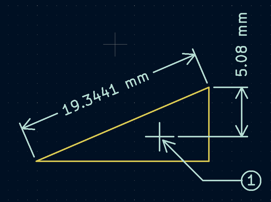
创建一个尺寸标注后,可以编辑其属性(快捷键 E)以改变显示数字的格式以及文本和图形线的风格。
| You can customize the default style of newly-created dimension objects in the Text & Graphics Defaults section of the Board Setup dialog. |
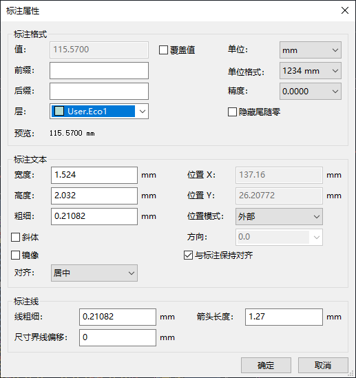
尺寸标注格式选项
覆盖值: 启用后,您可以直接在 值 字段中输入测量值,而不是实际测量值。
前缀: 此处输入的任何文字都将显示在测量值之前。
后缀: 此处输入的任何文字都将显示在测量值之后。
图层: 选择尺寸标注对象存在于哪个图层。
单位: 选择显示测量值的单位。 当更改电路板编辑器的显示单位时,自动 单位会导致尺寸标注单位发生变化。
单位格式: 从几种内置的单位显示风格中选择。
精度: 选择要显示多少位的精度。
尺寸标注文本选项
大多数尺寸标注文本选项与其他图形文本对象的选项相同(见上面的图形对象部分)。 也有一些特殊的选项适用于尺寸标注文本:
定位模式:选择是手动定位尺寸标注文本,还是自动保持与尺寸测量线对齐。
Keep aligned with dimension: When enabled, the orientation of the dimension text will be adjusted automatically to keep the text parallel with the measurement axis.
尺寸标注线选项
线条粗细: 设置构成标注形状的图形线的粗细。
Arrow length: Sets the length of the arrow segments of the dimension’s shape. A negative arrow length reverses the arrow direction.
延长线偏移:设置从测量点到延长线起点的距离。
Extension line overshoot: Sets the distance from the dimension’s line to the end of the extension lines.
引线选项
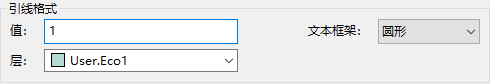
值: 输入要在引线行末尾显示的文本。
文本框: 选择所需的文本周围的边界(圆形、矩形或无)。
批量编辑文本和图形
Properties of text and graphics can be edited in bulk using the Edit Text and Graphics Properties dialog (Edit → Edit Text & Graphic Properties…).
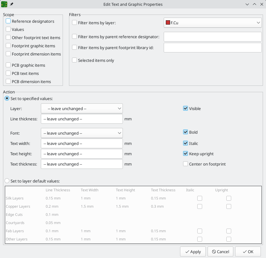
范围和筛选器
范围 设置限制了该工具只能编辑某些类型的对象。如果没有选择任何作用域,就不会有任何东西被编辑。
筛选器 限制该工具在选定的范围内编辑特定的对象。只有当对象符合所有启用的相关筛选器时才会被修改(有些筛选器不适用于某些类型的对象。例如,父封装筛选器不适用于图形项目,在改变图形属性时被忽略)。如果没有启用筛选器,所选范围内的所有对象都将被修改。对于带有文本框的筛选器,支持通配符。* 匹配任何字符,? 匹配任何单个字符。
按层筛选对象 筛选到指定板层上的对象。
按位号筛选对象 筛选到封装中具有特定位号的字段。通过父系封装库 ID 筛选对象 筛选到封装中具有指定库标识符的字段。
Selected items only filters to the current selection.
操作
被筛选对象的属性可以在对话框的底部设置为新的值。通过选择 设置为指定值,可以将属性设置为任意值,或者通过选择 设置为图层默认值,将属性重置为其图层的默认值。
下拉列表和文本框可以被设置为 --保持不变-- 以保留现有值。复选框可以被选中或不被选中,以启用或禁用某个变化,但也可以切换到第三种 "保持不变" 状态。
所有项目都可以设置其 层。
图形对象可以修改其 线的粗细。
Text properties that can be modified are font, text width, text height, text thickness (KiCad font only), emphasis (bold and italic), orientation (keep upright), and alignment (center on footprint). Footprint text can also have its visibility set.
Cleaning up graphics
There is a dedicated tool for performing common cleanup operations on graphics, which is run via Tools → Cleanup Graphics….
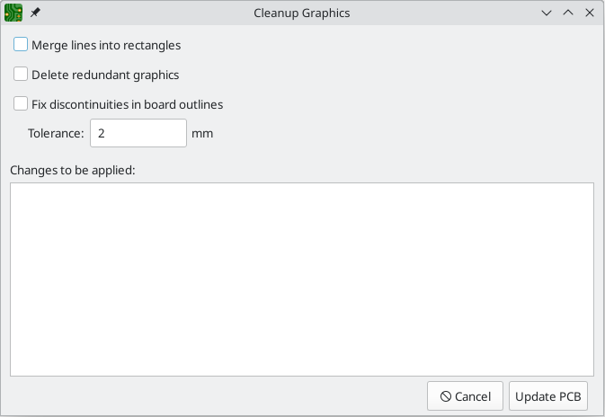
The following cleanup actions are available and will be performed when selected:
Merge lines into rectangles: combines individual graphic lines that together form a rectangle into a single rectangle shape object.
Delete redundant graphics: deletes graphics objects that are duplicated or degenerate.
Fix discontinuities in board outlines: modifies the existing board outline to fix any discontinuities that are within the specified tolerance.
Any changes that will be applied to the board are displayed at the bottom of the dialog. They are not applied until you press the Update PCB button.
Rule Areas (Keepouts)
Rule areas, also known as keepouts, are board regions that can have specific DRC rules defined for them. Some basic rules are available that will raise DRC errors if certain types of objects are within the bounds of the rule area, but rule areas can also be used together with custom DRC rules to define complex DRC behavior that only applies within the rule area.
You can add a rule area by clicking the ![]() button on the right toolbar (Ctrl+Shift+K). Click on the canvas to place the first corner, which will show the Rule Area Properties dialog. After configuring the rule area appropriately, press OK to continue placing corners of the rule area. The rule area shape can be an arbitrary polygon; click on the starting corner or double click to finish placing the rule area.
button on the right toolbar (Ctrl+Shift+K). Click on the canvas to place the first corner, which will show the Rule Area Properties dialog. After configuring the rule area appropriately, press OK to continue placing corners of the rule area. The rule area shape can be an arbitrary polygon; click on the starting corner or double click to finish placing the rule area.
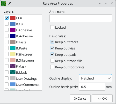
The Rule Area Properties dialog has the following options:
The layers list determines which layers the rule area applies to. The area only appears on these layers and the selected keepout rules only apply on these layers. At least one layer must be selected. By default, the active layer in the editing canvas is preselected in the rule area layer list.
The area name field is optional and provides an identifier for the rule area. If it is provided, it is included in DRC violation messages to make them clearer. It can also be used in custom DRC rules to identify a particular rule area.
The locked checkbox determines if the rule area should be locked. As with other objects, rule areas can also be locked or unlocked after they are created.
Several basic rules are available to keep out various types of objects. The basic rules can be configured to keep out tracks, vias, pads, zone fills, and/or footprints. If an object of one of the selected types is within the rule area, a DRC error will be raised. Additionally, zone fills will automatically avoid a rule area if the rule area is configured to keep out zones.
| Even with no basic rules selected, rule areas can still be used to define specific areas in which to apply custom DRC rules. |
There are a few options for the outline display of the rule area. The area can be shown with a hatched outline, fully hatched throughout the area, or with just the outline with no hatching. The outline hatch pitch is also adjustable.
向前和向后批注
从原理图更新 PCB(正向批注)
使用 "从原理图更新 PCB" 工具将设计信息从原理图编辑器同步到电路板编辑器。在原理图编辑器和电路板编辑器中都可以用 工具 → 从原理图更新 PCB(F8)来访问该工具。你也可以使用电路板编辑器顶部工具栏上的 ![]() 图标。这个过程通常被称为正向批注。
图标。这个过程通常被称为正向批注。
| 从原理图更新 PCB 是将设计信息从原理图转移到 PCB 的首选方法。在旧版本的 KiCad 中,相应的过程是将网表从原理图编辑器中导出并导入到电路板编辑器中。现在已经没有必要使用网表文件了。 |
该工具将每个符号的封装添加到电路板上,并将更新的原理图信息传输到电路板上。尤其重要的是,电路板的网络连接也将更新以匹配原理图。
将对 PCB 进行的变更列在 待应用的变更 窗格中。在你点击 更新 PCB 按钮之前,PCB 不会被修改。
你可以使用窗口底部的复选框来显示或隐藏不同类型的信息。可以使用 保存… 按钮将变更的报告保存到文件中。
选项
该工具有几个选项来控制其行为。
| 选项 | 描述 |
|---|---|
根据位号将封装重新链接到原理图符号上 |
封装通常是通过符号添加到原理图中时创建的唯一标识符与原理图符号相连。符号的唯一标识符不能被改变。 如果选中,PCB 中的每个封装将被重新链接到与该封装具有相同位号的符号上。 如果不勾选,封装和符号将像往常一样通过唯一的标识符来链接,而不是通过位号。每个封装的位号将被更新以匹配其链接符号的位号。 这个选项一般不应该被选中。它对依赖改变原理图符号和封装之间的链接的特定工作流程很有用,例如重构原理图以方便布局,或者在设计的相同通道之间复制布局。 |
删除没有符号的封装 |
如果选中,PCB 中任何在原理图中没有相应符号的封装都将从 PCB 中删除。带有 "不在原理图中" 属性的封装将不受影响。 如果不勾选,没有相应符号的封装将不会被删除。 |
用原理图中指定的封装替换封装 |
如果选中,PCB 中的封装将被替换为相应原理图符号中指定的封装。 如果不勾选,即使原理图符号被更新为指定了不同的封装,PCB 中已有的封装也不会被改变。 |
从 PCB 更新原理图(反向批注)。
KiCad 的典型工作流程是在原理图中进行修改,然后使用 "从原理图更新 PCB" 工具将修改内容同步到电路板上。然而,相反的过程也是可行的:可以在电路板上进行设计修改,然后在原理图或电路板编辑器中使用 工具 → 从 PCB 更新原理图 同步到原理图上。这个过程通常被称为反向批注。
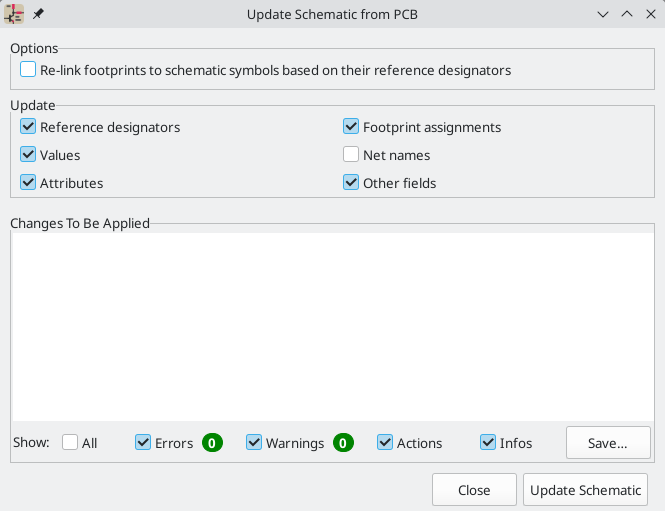
该工具将位号、值、封装分配和网络名称的变化从电路板同步到原理图。每种类型的变更都可以单独启用或禁用。
将对原理图进行的变更列在 待应用的变更 窗格中。在您点击 更新原理图 按钮之前,原理图不会被修改。
你可以使用窗口底部的复选框来显示或隐藏不同类型的信息。可以使用 保存… 按钮将变更的报告保存到文件中。
选项
该工具有几个选项来控制其行为。
Option |
Description |
Re-link footprints to schematic symbols based on their reference designators |
If checked, each footprint in the PCB will be re-linked to the symbol that has the same reference designator as the footprint. This option is incompatible with updating symbol reference designators. If unchecked, footprints and symbols will be linked by unique identifier as usual, rather than by reference designator. |
Reference designators |
If checked, symbol reference designators will be updated to match the reference designators of the linked footprints. If unchecked, symbol reference designators will not be updated. |
Values |
If checked, symbol values will be updated to match the values of the linked footprints. If unchecked, symbol values will not be updated. |
Footprint assignments |
If checked, footprint assignments will be updated for symbols which have had their footprints changed or replaced in the board. If unchecked, symbol footprint assignments will not be updated. |
Net names |
If checked, the schematic will be updated with any net name changes that have been made in the board. Net labels will be updated or added to the schematic as necessary to match the board. If unchecked, net names will not be updated in the schematic. |
| 按位置重新批注 功能可以与反向批注位号结合使用,根据设计中的位置重新批注所有元件。 |
用 CMP 文件进行反向批注
通过从 PCB 编辑器导出 CMP 文件(文件 → 导出 → 封装关联(.cmp)文件…)并在原理图编辑器中导入(文件 → 导入 → 封装分配…),也可以将选择的变化从 PCB 上同步到原理图。
| 这种方法只能同步对封装分配和封装字段的修改。建议使用 "从 PCB 更新原理图" 工具来代替。 |
按位置重新批注
The Geographical Reannotation tool lets you automatically set the reference designators of footprints based on their physical location on the board.
To run the Geographical Reannotation tool, use Tools → Geographical Reannotate…. This opens the geographical reannotation dialog with options for how to perform the reannotation.
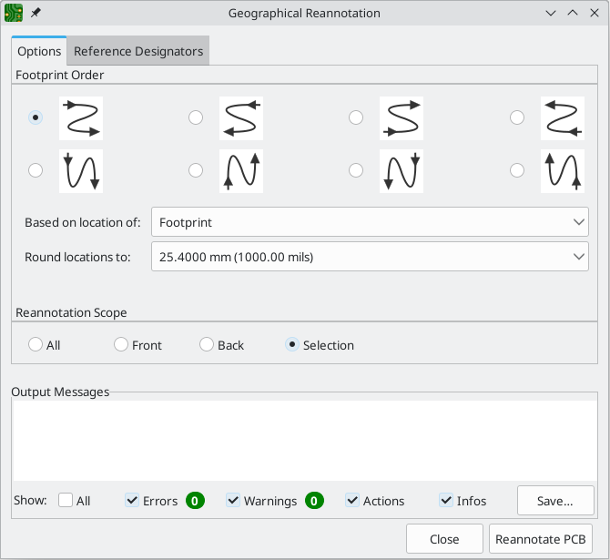
The Options tab contains settings for how footprint locations affect reannotation. The arrow diagrams indicate which geographical ordering to use when reannotating. You can reannotate from left-to-right, right-to-left, top-to-bottom, or bottom-to-top, and you can select whether to use a column-major order (go through all footprints in the same column before moving to the next column) or row-major order (go through all footprints in the same row before moving to the next row).
Geographical reannotation can either use the location of the footprint itself or the location of the footprint’s reference designator. You can also select how much to round footprint locations before determining which footprints are at the same X or Y position. Rounding to a finer coordinate resolution will result in fewer footprints considered to be in the same row or column.
Finally, you can select which footprints to reannotate. You can reannotate all footprints on the board, all footprints on the front or back of the board, or all footprints in your selection.
The Reference Designators tab contains options for how to allocate new reference designators. There are separate settings for footprints on the front and back of the board.
Reference start controls the number for the first new reference designator on each side of the board. If no start value is given for the back of the board, back side footprints will be annotated starting at one higher than the last front side reference designator.
Prefix specifies a prefix string to insert at the beginning of each newly assigned reference designator. This prefix will be inserted before any prefix that is already present. If the remove prefix option is selected, footprints with the specified prefix will instead have that prefix removed instead of added. Footprints without that prefix will not have not have any prefix added or removed.
If exclude locked footprints is checked, locked footprints will not be reannotated. You can also avoid reannotating specific footprints by entering their reference designators as a comma-separated list in the exclude references box.
When you click the Reannotate PCB button, footprints will be reannotated according to the selected settings.
| The Geographical Reannotation tool updates reference designators in the board, but not in the schematic. After geographically reannotating the board, be sure to sync the updated reference designators to the schematic by running the Update Schematic from PCB tool with the re-link footprints to schematic symbols based on their reference designators option disabled. If the schematic is not updated, reference designators in the board will not match those in the schematic. |
锁定
大多数对象可以通过其属性对话框、右键上下文菜单或使用 "切换锁定" 快捷键(L)来锁定。 被锁定的对象不能被选择,除非选择过滤器中的 "被锁定的项目" 复选框被启用。 试图移动锁定的项目将导致一个警告对话框:
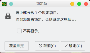
在这个对话框中选择 "覆盖锁定" 将允许移动锁定的项目。 选择 "确定" 将允许你在选中对象中移动任何未上锁的对象;留下锁定的对象。 选择 "不再显示" 将使你在剩下的会话中记住你的选择。
Locked items are displayed with a colored shadow around them. This can be customized in your color scheme.
Groups
Groups let you treat multiple objects as a single object for the purposes of moving or rotating them. Each object in the group will maintain its position relative to the other objects in the group. Groups can also have a name, which is displayed in the editing canvas when the group is selected.
Most types of objects in the Board Editor can be grouped: footprints, tracks, zones, graphic items, and even other groups. Groups can contain multiple different types of objects at once.
To add objects to a group, select them, then right click and choose Grouping → Group Items. To remove all items from a group, select the group, right click, and choose Grouping → Ungroup Items.
Once objects have been added to a group, selecting any of the objects will select the group as a whole instead of the constituent objects. To edit a specific object within a group, first select the group, the right click and choose Enter Group. Double clicking on a group also enters the group. When a group has been entered, objects within the group can be selected and edited individually without affecting the other objects in the group. To leave the group and stop editing its members individually, right click and select Leave Group, select an object outside the group, or use Esc.
There are several ways to modify which objects belong to a group. To remove objects from an existing group, enter the group, then select the objects you want to remove, right click, and choose Grouping → Remove Items. To add items to a group, first ungroup all the items from the group. This will leave the group’s former members selected. Then add the new item to the selection and group the selection. Note that without first ungrouping, this process would create a nested group: a new group containing the new item and the entire original group, not just the items in the original group.
You can also add or remove objects from a group in the group’s properties dialog. To open a group’s properties dialog, press E or right click and click Properties…. The properties dialog lists the objects contained in the group. To add an additional object to the group, click the ![]() button, then click on the desired object in the editing canvas. The object you click on will be added to the group. To remove an object, select it in the list, then click the
button, then click on the desired object in the editing canvas. The object you click on will be added to the group. To remove an object, select it in the list, then click the ![]() button.
button.
The group properties dialog also lets you specify a name for the group or lock the group. Groups can also be named or locked using the properties manager.
Creating Arrays
KiCad has an array tool to create rectangular or circular arrays of objects (footprints, vias, graphical objects, etc.). Two types of array are possible: Grid and Circular.
Grid Arrays are rectangular and are described by a horizontal count and a vertical count, which set the number of columns and rows in the array, respectively. The horizontal and vertical spacing settings describe the distance between columns and rows, while the horizontal and vertical offset settings describe a shift applied to each row/column compared to the previous row/column.
You can create a repeating staggered pattern by choosing a stagger setting, which controls the number of rows or columns that are offset before the pattern repeats. You can stagger by row or by column. For example, if two staggered rows are selected, each row will be horizontally offset from the previous row by half of the array’s horizontal spacing setting. Every other row will be placed at the original spacing and offset. If three staggered columns are selected, each column will be vertically offset by a third of the array’s vertical spacing setting. Every third column will be placed at the original spacing and offset. Offsets from the stagger settings are added to the previous horizontal and vertical offset settings.
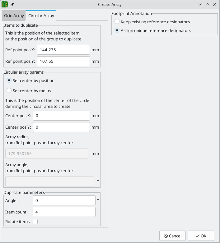
Circular Arrays are described by a center point, an angular spacing, and a number of arrayed items. If set center by position is selected, the center point of the array will be defined by the absolute X/Y position you enter in center pos X and center pos Y. If set center by radius is selected, the center point of the array will be defined by the array radius and array angle parameters, which describe the position of the array center relative to the source object’s position. The source object’s position is displayed for reference as ref point pos X and ref point pos Y.
The item count field determines the number of objects in the array, including the source object. The angle field determines the angular spacing between items, with the center point at the center of the array. Positive angles result in a counter-clockwise rotation relative to the center point and the source item, while negative angles result in a clockwise rotation. An angle of 0 will result in a complete circle with objects evenly spaced to provide the specified number of objects. If the item count is too small to create a full circle with the specified spacing between objects, the array will not be a complete circle. When rotate items is selected, objects will be rotated around their origins as array sweeps around the center point. Otherwise, objects will maintain the same orientation as the source item.
When creating an array of footprints, whether rectangular or circular, the Footprint Annotation settings control how the reference designators will be set in the new footprints. This affects the linkage of the new footprints to the schematic. If keep existing reference designators is selected, the new footprints in the array will have the same reference designators as the source footprints, resulting in duplicated reference designators in the board. If assign unique reference designators is selected, each new footprint created in the array will have a unique reference designator automatically assigned.
| Creating an array of footprints will result in multiple copies of the source footprint(s). If you are using a schematic-based workflow, this will result in footprints that are not represented in the schematic, so careful syncing between the board and the schematic will be needed. |
After creating an array, the newly added objects remain selected (not including the original source object), which allows you to easily delete the array if the parameters need to be adjusted.
清理工具
| KiCad文档的这一部分还没有写。 我们 我们感谢您的耐心等待,因为我们的志愿文档编写小队 撰写者组成的小团队正在努力更新和扩展文档,我们感谢您的耐心等待。 |
从 DXF 和 SVG 文件导入矢量图
| KiCad文档的这一部分还没有写。 我们 我们感谢您的耐心等待,因为我们的志愿文档编写小队 撰写者组成的小团队正在努力更新和扩展文档,我们感谢您的耐心等待。 |
Using reference images
KiCad supports displaying reference images in the canvas. These are background images that you can use to help you lay out a board; they are purely for reference during the design process and are not included in any fabrication outputs.
To add a reference image, use the ![]() button on the right toolbar and select the desired reference image file.
button on the right toolbar and select the desired reference image file.
Once the image has been added to the canvas, you can scale it by dragging the editing canvas or open its properties dialog (E) and set the scale explicitly in the Image tab. Here you can also Convert to Greyscale if you wish.
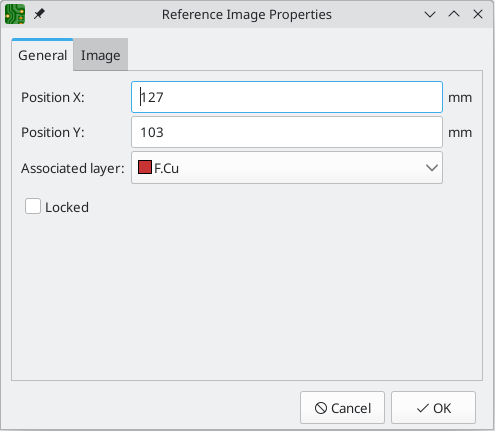
Reference images have an associated layer; they are shown and hidden along with this layer. The layer initially associated with a reference image is the layer that was active when the image was added. You can change the associated layer in the image’s properties.
Another way to hide reference images is with the appearance manager. You can show or hide all reference images by toggling the visibility of Image objects in the Objects tab (![]() button). You can also adjust the opacity of reference images here.
button). You can also adjust the opacity of reference images here.
检查电路板
测量工具
测量工具允许你在 PCB 上的各点之间进行距离和角度测量。 要激活该工具,请点击右侧工具栏的 ![]() 图标,或使用快捷键 Ctrl+Shift+M。 一旦该工具被激活,点击一次以设置测量起点,然后再点击一次以完成测量。
图标,或使用快捷键 Ctrl+Shift+M。 一旦该工具被激活,点击一次以设置测量起点,然后再点击一次以完成测量。
| 测量工具用于不需要永久显示的快速测量。 您所做的任何测量都将仅在该工具处于活动状态时显示。 要创建将显示在打印输出和打印中的永久性尺寸标注,请使用尺寸标注工具。 |
设计规则检查
设计规则检查器用于验证 PCB 是否符合 “电路板设置” 对话框中建立的所有要求,以及所有焊盘是否按照网表或原理图连接。 KiCad 可以在布线时自动防止一些违反设计规则的行为,但许多其他的行为是无法自动防止的。 这意味着在为 PCB 生成制造文件之前,必须使用设计规则检查器。
要使用设计规则检查器,请点击顶部工具栏的 ![]() 图标,或从 检查 菜单中选择 设计规则检查器。
图标,或从 检查 菜单中选择 设计规则检查器。
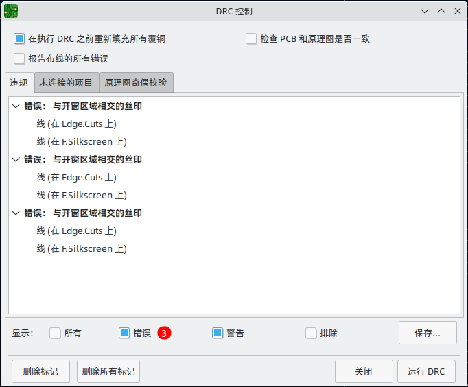
DRC 控制窗口的顶部部分包含一些控制设计规则检查器的选项:
重新敷铜后再执行 DRC: 启用后,每次运行设计规则检查器时都会重新敷铜。 如果未手动重新敷铜,禁用此选项可能会导致错误的 DRC 结果。
报告每个布线的所有错误: 启用后,将报告每个布线的所有间隙错误。 禁用时,将只报告第一个错误。 启用此选项将导致设计规则检查器运行速度变慢。
测试 PCB 和原理图之间的一致性(parity): 启用后,设计规则检查器除了测试 PCB 设计规则外,还将测试原理图和 PCB 之间的差异。 在独立模式下运行 PCB 编辑器时,该选项不起作用。
运行 DRC 后,任何违规行为都会显示在 “DRC 控制” 窗口的中间部分。 违反规则、未连接的项目以及原理图和 PCB 之间的差异会显示在三个不同的标签中。 违规列表下面的控件可以用来显示或隐藏违规,这取决于其严重程度。 在运行 DRC 后,可以使用保存按钮创建一个纯文本格式的报告文件。
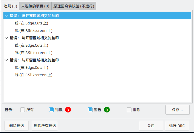
每个违规行为都涉及 PCB 上的一个或多个对象。 在违规列表中,涉及的对象列在违规行为下面。 点击列表中的违规行为将移动 “PCB 编辑器” 的视图,使受影响的区域居中。 点击违规所涉及的对象之一将高亮显示该对象。
窗口底部的数字显示错误、警告和排除的数量。每种类型的违规行为都可以用各自的复选框从列表中过滤出来。点击 删除标记 将清除所有违规行为,直到再次运行 DRC。
可以在对话框中右键单击违规行为,以忽略它们或改变其严重程度:
-
排除此违规行为: 忽略此特定的违规行为,但不影响任何其他违规行为。
-
更改严重程度: 将一个违规类型从警告改为错误,或将错误改为警告。这影响到一个给定类型的所有违规行为。
-
忽略所有: 忽略所有给定类型的违规。这个测试现在将出现在 忽略的测试 标签,而不是 违规 标签。
在设计规则检查器运行期间,排除的和忽略的违规行为会被记住。
间隙和约束解析
间隙和约束解析工具允许你检查哪些间隙和设计约束规则应用于选定的项目。 当设计具有复杂设计规则的 PCB 时,这些工具可以提供帮助,因为在这种情况下并不总是清楚哪些规则适用于哪些对象。
要检查两个对象之间适用的间隙规则,选择这两个对象并从 检查 菜单中选择 间隙解析。 间隙报告对话框将显示每个铜层上的对象之间所需的间隙,以及产生该间隙的设计规则。
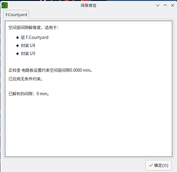
要检查适用于单一对象的设计约束,选择它并从 检查 菜单中选择 约束解析。 约束报告对话框将显示适用于该对象的所有约束。
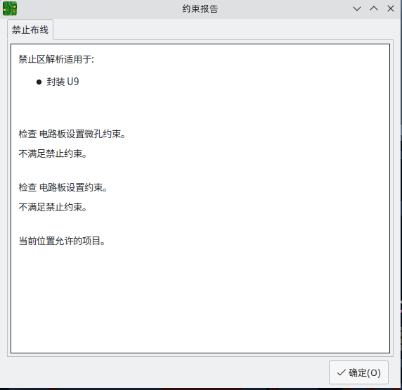
Board Statistics
The Board Statistics dialog shows a summary of the board’s contents, including the number of components, pads and vias; each by their own types as well as the overall board size.
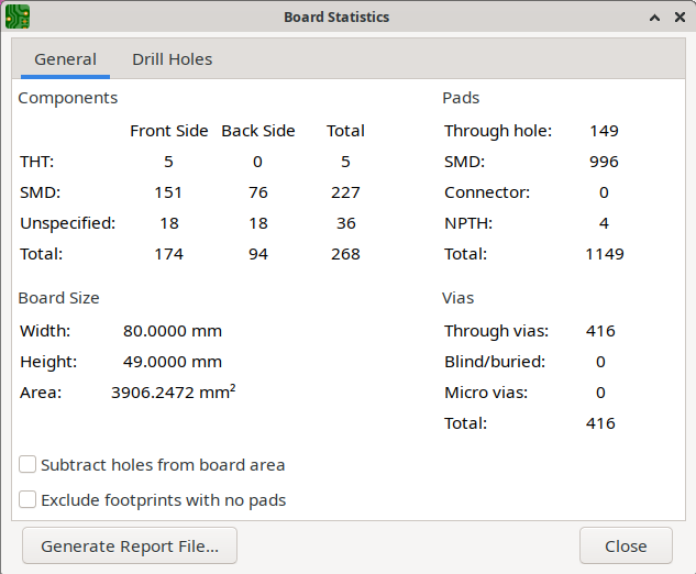
查找工具
查找工具在 PCB 中搜索文本,包括位号、封装字段和图形文本。当该工具找到一个匹配的文本时,画布会被放大,并将其置于匹配文本的中心位置,同时文本被高亮显示。使用顶部工具栏中的(![]() )按钮启动该工具。
)按钮启动该工具。
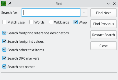
查找工具有几个选项:
匹配大小写: 选择搜索是否对大小写敏感。
关键词: 当选择时,搜索将只与 PCB 中的完整单词相匹配。当未选择时,如果搜索词是 PCB 中一个较长的词的一部分,搜索将匹配。
通配符: 当选择时,通配符可以在搜索词中使用。? 匹配任何单个字符,* 匹配任何数量的字符。请注意,当选择这个选项时,不会返回部分匹配结果:搜索 abc* 将匹配字符串 abcd,但搜索 abc 则不会。
Wrap: 选中时,搜索结果将在到达最后一个匹配项后返回到第一个匹配项。
搜索封装位号: 选择搜索是否应适用于封装位号。
搜索封装值: 选择搜索是否应适用于封装值字段。
搜索其他文本项目: 选择搜索是否应适用于其他文本项目,包括图形文本以及除了值和位号之外的封装字段。
搜索 DRC 标记: 选择搜索是否应适用于电路板上显示的 DRC 标记的违规描述。
Search net names: Selects whether the search should apply to the names of nets in the board.
搜索面板
The search panel is a docked panel that lists information about footprints, zones, nets, ratsnest lines (unrouted segments), and text from the PCB. You can optionally filter the list based on a search string. When no filter is used, all items in the design are listed in the corresponding tab.
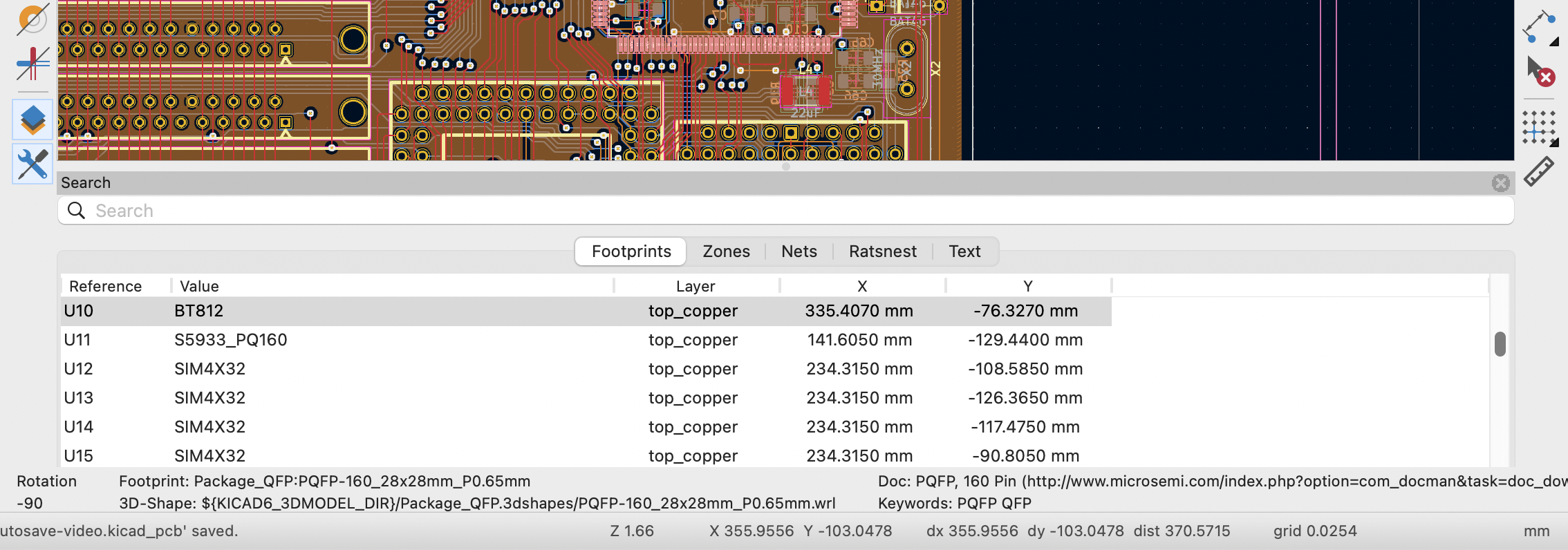
Items are filtered based on their properties: footprints are filtered by their reference designator and value, zones by the zone name, net and ratsnest items by the net name, and text (text, textboxes, and dimensions) by the text content. You can sort the filtered results in ascending or descending order of the value in a particular column by clicking on that column header.
Filters support wildcards: * matches any characters, and ? matches any single character. You can also use regular expressions, such as /footprint value/.
The displayed information depends on the item type. In addition to the item’s name and/or value, physical items (footprints, zones, and text) list their layer and X/Y location. Text also displays the type of text object (text, textbox, or dimension.) Net and ratsnest items list their net name and net class.
When you click an item in the search panel, the item is selected in the editing canvas. Double-clicking an item in the search panel opens its properties dialog (for net and ratsnest items, the net classes dialog is opened instead).
Show or hide the search panel with View → Show Search Panel or use the Ctrl+G shortcut.
3D 查看器
The 3D Viewer shows a 3-dimensional view of the board and the components on the board. You can view the board from different perspectives, show or hide different types of components, cross-probe from the PCB Editor to the 3D viewer, and generate raytraced renders of the board. Show the 3D Viewer with View → 3D Viewer or use the Alt+3 shortcut.
| 仅当 3D 模型文件存在并且已被 分配到封装 时,元件的 3D 模型才会出现。 |
| KiCad 标准库中的许多封装还没有为它们创建模型文件。然而,这些封装可能包含一个指向尚不存在的 3D 模型的路径,以期待将来创建 3D 模型。 |
浏览 3D 视图
用鼠标左键拖动将旋转 3D 视图。 默认情况下,这是电路板的中心,但可以通过将光标移动到所需点上并按 Space 将轴心点重置为电路板上的新点。 滚动鼠标滚轮将放大或缩小视图。 按住 Ctrl 滚动可左右平移视图,按住 Shift 滚动可上下平移视图。 使用鼠标中键拖动也可以平移视图。
Different sized 3D grids can be set using the View → 3D Grid menu. Bounding boxes for each component can be enabled with Preferences → Show Model Bounding Boxes.
当 PCB 编辑器和 3D 查看器同时打开时,在 PCB 编辑器中选择一个封装也会在 3D 查看器中高亮显示该元件。高亮显示的颜色可以在 偏好设置 → 偏好设置… → 3D 查看器 → 实时渲染器 → 选择颜色 中调整。
Appearance manager
The appearance manager is a panel at the right of the viewer which provides controls to manage the visibility, color, and opacity of different types of objects and board layers in the 3D view.
Each layer or type of object in the list can be individually shown or hidden by clicking its corresponding visibility icon. PCB layers can have their colors customized; double-click on the color swatch next to the item type to edit the item’s color and opacity. To use the colors selected in the Board Setup dialog’s Physical Stackup editor, enable the use board stackup colors option.
You can save an appearance configuration as a preset, or load a configuration from a preset, using the Preset selector at the bottom. The Ctrl+Tab hotkey cycles through presets; press Tab repeatedly while holding Ctrl to cycle through multiple presets. Several built-in presets are available: "Follow PCB Editor" matches the visibility settings in the PCB editor, "Follow PCB Plot Settings" matches the visibility settings selected in the Plot dialog, and "legacy colors" matches the default 3D Viewer color settings from older versions of KiCad.
Finally, you can save a viewport for later retrieval using the Viewports selector at the bottom. You can quickly cycle between saved viewports using Shift+Tab; pressing Tab repeatedly while holding Shift will cycle through multiple viewports.
用 3D 查看器生成图像
当前的 3D 视图可以用 文件 → 将当前视图导出为 PNG… 或 将当前视图导出为 JPG…,根据所需的图像格式,将其保存为一个图像。也可以用 ![]() 按钮,或 编辑 → 复制 3D 图像 将当前视图复制到剪贴板上。
按钮,或 编辑 → 复制 3D 图像 将当前视图复制到剪贴板上。
3D 查看器有一个光线跟踪渲染模式,它使用比默认渲染模式更精确的物理渲染模型来显示电路板。 光线追踪比默认渲染模式慢,但当需要最吸引人的视觉效果时,可以使用它。使用 ![]() 按钮,或者使用 偏好设置→光线追踪 来启用光线追踪模式。在光线追踪模式下,3D 网格和选择高亮不会显示。
按钮,或者使用 偏好设置→光线追踪 来启用光线追踪模式。在光线追踪模式下,3D 网格和选择高亮不会显示。
颜色和其他渲染选项,包括光线跟踪和非光线跟踪模式,都可以在 偏好设置 → 偏好设置… → 3D查看器 中调整。
3D 查看器控制
许多查看选项是通过顶部的工具栏控制的。
|
Reload the 3D model |
|
Copy 3D image to clipboard |
|
Render current view using raytracing |
|
Redraw |
|
Zoom in |
|
Zoom out |
|
Fit drawing in display area |
|
Rotate X clockwise |
|
Rotate X counterclockwise |
|
Rotate Y clockwise |
|
Rotate Y counterclockwise |
|
Rotate Z clockwise |
|
Rotate Z counterclockwise |
|
Flip board view |
|
Pan board left |
|
Pan board right |
|
Pan board up |
|
Pan board down |
|
Enable/disable orthographic projection |
|
Show/hide the appearance manager |
网络检查
The Net Inspector allows you to view statistics about all the nets in a board. To open the inspector, click the ![]() icon at the top of the Nets section of the Appearance panel, or select Net Inspector from the Inspect menu.
icon at the top of the Nets section of the Appearance panel, or select Net Inspector from the Inspect menu.
点击网络列表中的一个网络会在电路板上高亮显示该网络。 单击列标题允许您按该列对网络列表进行排序。
The Group By field allows you to combine different nets together and view the total length of the combined nets. For example, if you have two nets named DATA0 and DATA0_EXT, using a Group By value of DATA0* will create a group containing both nets. More complicated groupings can be created by changing the Group By mode from Wildcard to RegEx (regular expressions). The substring (Substr) variants of the Group By mode will create groups for each set of nets that matches the pattern differently.
例如,如果您有 U1D+,U1D-,U2D+ 和 U2D-,分组模式 U*D 将在通配符模式下匹配所有四个网络,创建一个单一的组 U*D。 在通配符子串模式下,它将匹配所有四个网络,但创建两个不同的组:U1D 和 U2D。
焊盘计数 和 过孔计数 显示一个网络的焊盘(表面贴装和通孔)及过孔的数量。 过孔长度 显示每个过孔的总高度(不考虑过孔连接到哪个铜层)。 换句话说,过孔长度等于过孔数乘以电路板的层叠高度。 布线长度 显示一个网络中所有布线的总长度,不考虑拓扑结构。 晶圆长度 显示了网络中所有焊盘设置的 “晶圆到焊盘长度“ 值的总和。
Differences between Net Inspector and Length Tuner
The Net Inspector may report different net lengths than the length tuner, because the two tools have different purposes and calculate track/net lengths differently. In short, the Net Inspector sums up the total length of each track segment and via on a net, while the length tuner calculates the effective electrical length of a path between two points on a net. The specific differences are as follows:
-
The Net Inspector reports track length as a simple sum of the length of each track segment on a net. The length tuner calculates an effective electrical length of a net, which includes optimizing paths through pads to calculate the shortest possible path.
-
If a routed net has a branching topology, the Net Inspector total includes the length of each branch in the total. The length tuner calculates a point-to-point length; if there are any branches, the length tuner will stop at the closest branch and report the length up to the branch.
-
The Net Inspector always uses the full via height, from the front layer to the back layer, for its via length and total length calculations. The length tuner does not necessarily use the full via height, depending on which layers the tuned net occupies. If use stackup height is enabled in the board constraint settings, the length tuner will use the stackup information to include only the length of the portion of the via between the two relevant signal layers. If use stackup height is not enabled, the length tuner will not include vias in its calculations at all.
生成输出
KiCad 可以生成和导出多种不同格式的文件,这些文件对制造 PCB 和与外部软件的接口很有用。 该功能可在文件菜单的几个不同部分中找到。 制造输出部分包含准备制造 PCB 所需的最常见操作。 输出部分包含生成可由外部软件读取的文件的工具。 绘图功能允许你以各种格式导出 PCB 的 2D 绘图。 打印功能允许你将 PCB 的视图发送到 2D 打印机上。
制造输出和绘图
KiCad uses Gerber files as its primary plotting format for PCB manufacturing. To create Gerber files, open the Plot… dialog from the File menu, or select Gerbers (.gbr)… from the Fabrication Outputs section of the File menu. The Plot dialog will open, allowing you to configure and generate Gerber files.
绘图选项
包含层: 检查电路板上使用的每一个层在列表中是否被启用。 被禁用的图层将不会被绘制出来。
Plot on All Layers: Selected layers will be included in the plot for each layer selected in the include layers list. The additional layers are plotted on top of the base layer. You can reorder these layers using the arrow buttons at the bottom; items that are lower in the list are plotted after (on top of) items that are higher in the list.
输出目录: 指定打印文件的保存位置。 如果这是相对路径,则它是相对于工程目录创建的。
Plot drawing sheet: If enabled, the drawing sheet border and title block will be plotted on each layer. This should usually be disabled when plotting Gerber files.
绘制封装值: 如果启用,每个封装的值字段将绘制在其所在的任何层上 (除非特定封装的字段可见性被禁用)。
绘制位号: 如果启用,每个封装的位号字段将绘制在其所在的任何层上 (除非特定封装的字段可见性被禁用)。
Plot footprint text: If enabled, text fields in footprints will be plotted on whatever layers they exist on (unless the field visibility is disabled for a specific footprint). Disabling this option also disables the plot footprint values and plot reference designators options.
强制绘制不可见值/位号: 如果启用,将绘制所有封装值和位号,即使其中一些字段可见性被禁用。
在所有图层上绘制板边(Edge.Cuts): 如果启用,Edge.Cuts(电路板边框) 图层将添加到所有其他层。 请向您的制造商咨询,了解此设置对于其制造过程的正确值是多少。
制造层上的草图焊盘: 如果启用,制造 (F.Fab,B.Fab) 层上的封装焊盘将绘制为未填充的边框,而不是填充的形状。
绘制前检查敷铜区域: 启用后,将在生成输出之前检查敷铜 (如果过期则重新敷铜)。 如果禁用此选项,绘制输出可能不正确!
钻孔标记: 对于 Gerber 以外的绘图格式,可以在所有钻孔的位置绘制标记。 钻孔标记可以按成品孔的实际尺寸 (直径) 创建,也可以按较小的尺寸创建。
缩放: 对于支持非 1:1 缩放的打印格式,可以设置打印比例。 自动缩放设置将缩放绘图以适合指定的页面大小。
绘图模式: 对于某些绘图格式,填充的形状可能只被绘制成边框(草图模式)。
使用钻孔/拾放文件原点: 启用后,绘制文件的坐标原点将是电路板编辑器中设置的钻孔/拾放文件原点。 禁用时,坐标原点将是绝对原点 (图框的左上角)。
镜像绘图: 对于某些绘图格式,设置此选项后输出会水平镜像。
负片绘图: 对于某些绘制格式,可能会将输出设置为负片模式。 在此模式下,将为电路板边框内的空白区域绘制图形,并在 PCB 中存在对象的位置留下空白区域。
不允许过孔盖油: 如果启用,过孔将在阻焊层 (F.Mask、B.Mask) 上不会被覆盖。 如果禁用,过孔将被阻焊层 (绿油) 覆盖。
| KiCad 不支持指定过孔的盖油设置。 过孔盖油只能是全局控制的(一块板上的所有过孔)。 |
Gerber 选项
使用 Protel 文件扩展名: 启用后,绘制的 Gerber 文件将使用基于 Protel (.GBL、.GTL 等) 的文件扩展名命名。
当禁用时,文件将有 .gbr 的扩展名。
生成 Gerber 作业文件: 开启后,Gerber 作业文件 (.gbrjob) 将与任何 Gerber 文件一起生成。
Gerber 作业文件是 Gerber 格式的扩展,包括有关 PCB 层叠、材料和表面处理的信息。
有关 Gerber 工作文件的更多信息,请访问链接:Ucamco 网站。
Subtract soldermask from silkscreen: When enabled, silkscreen will be automatically removed from board areas that aren’t covered by soldermask.
坐标格式: 配置坐标在绘制的 Gerber 文件中的存储方式。 请咨询您的制造商,了解他们对此选项的推荐设置。
使用扩展的 X2 格式: 启用后,绘制的 Gerber 文件将使用 X2 格式,其中包括有关网表和其他扩展属性的信息。 此格式可能与某些制造商使用的旧版 CAM 软件不兼容。
包含网表属性: 启用后,绘制的 Gerber 文件将包含可用于在 CAM 软件中检查设计的网表信息。 禁用 X2 格式模式时,此信息将作为注释包含在 Gerber 文件中。
禁用孔径宏: 启用后,所有形状都将绘制为图元,而不是使用孔径宏。 此设置仅应在您的制造商要求时用于与旧的或有缺陷的 CAM 软件兼容。
Postscript 选项
缩放系数: 控制电路板文件中的坐标将如何被缩放到 PostScript 文件中的坐标。 使用不同的 X 和 Y 比例因子的值将导致输出的拉伸/扭曲。 这些系数可以用来纠正 PostScript 输出设备中的缩放比例,以实现精确的输出比例。
布线宽度校正: 在绘制 PostScript 文件时,从布线、过孔和焊盘的尺寸中添加(或减去,如果是负的)一个全局系数。 这个系数可用于纠正 PostScript 输出设备中的错误,以实现精确的比例输出。
强制 A4 输出: 启用后,生成的 PostScript 文件将为 A4 大小,即使 KiCad 电路板文件大小不同。
SVG 选项
精度: 控制将使用多少个有效数字来存储坐标。
Output mode: Controls whether the generated SVG file is in color or black and white.
DXF 选项
使用图形项目的轮廓线绘图: DXF 文件中的图形形状没有宽度。 此选项控制如何将 KiCad 电路板中具有宽度 (厚度) 的图形绘制到 DXF 文件。 启用此选项后,将绘制图形的外边框。 禁用此选项时,将绘制图形的中心线 (并且形状的厚度在生成的 DXF 文件中不可见)。
使用 KiCad 字体绘制文本: 启用后,KiCad设计中的文本将被绘制成使用KiCad字体的图形。 禁用时,文本将作为 DXF 文本对象绘制,它将使用不同的字体,并且不会以与 KiCad 电路板编辑器中显示的完全相同的位置和大小显示。
导出单位: 控制将在 DXF 文件中使用的单位。 由于DXF格式没有指定的单位系统,你必须使用与你想在其他软件中使用的相同的单位设置来输出。
HPGL 选项
默认笔尺寸: 控制用于创建图形的绘图仪笔尺寸。
PDF options
Output mode: Controls whether the generated PDF file is in color or black and white.
Generate property popups for front footprints: When enabled, interactive popups will be added to the generated PDF containing part information for each footprint on the front of the board.
Generate property popups for back footprints: When enabled, interactive popups will be added to the generated PDF containing part information for each footprint on the back of the board.
钻孔文件
KiCad can generate CNC drilling files required by most PCB manufacturing processes in either Excellon or Gerber X2 format. KiCad can also generate a drill map: a graphical plot of the board showing drill locations. Select the Drill Files (.drl)… option from the Fabrication Outputs section of the File menu to open the dialog:
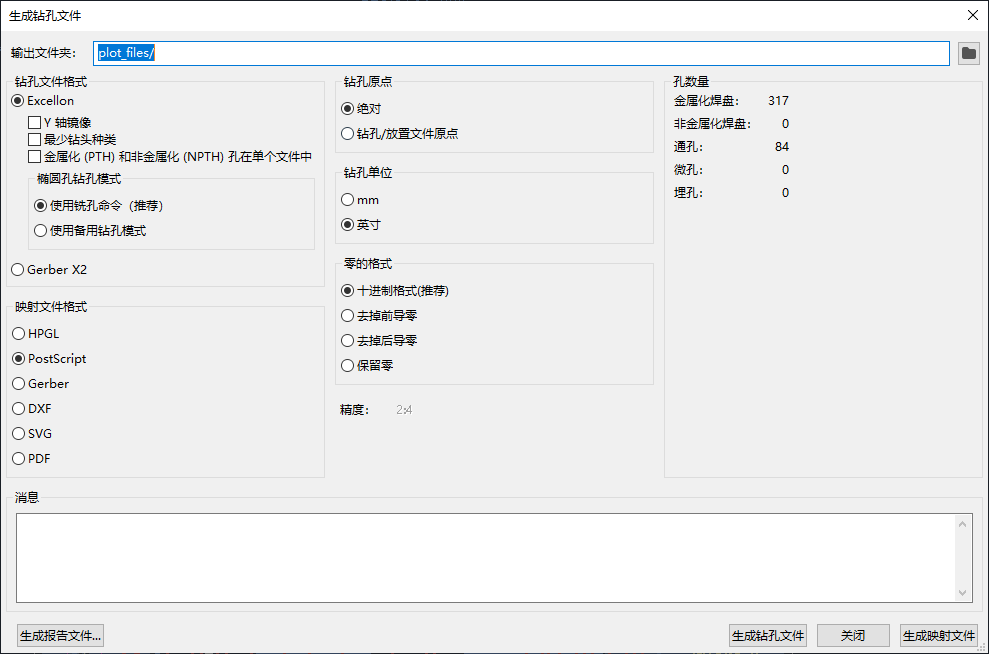
输出文件夹: 选择要保存生成的钻孔和映射文件的文件夹。 如果输入一个相对路径,则将是相对于工程目录的。
钻孔文件格式: 选择是生成 Excellon 钻孔文件 (大多数 PCB 制造商都需要)还是 Gerber X2 文件。
镜像 Y 轴: 对于 Excellon 文件,选择是否镜像 Y 轴坐标。 当由第三方制造 PCB 时,通常不应使用该选项。这仅是为了方便自己制造 PCB 的用户而提供的。
最小文件头: 对于 Excellon 文件,选择是否输出最小文件头,而不是完整的文件头。 除非制造商要求,否则不应启用此选项。
PTH (电镀孔) 和 NPTH (非电镀孔) 在同一文件中: 默认情况下,会在两个不同的 Excellon 文件中生成电镀孔和非电镀孔。 启用此选项后,这两个文件将合并为单个文件。 除非制造商要求,否则不应启用此选项。
椭圆孔钻孔模式: 控制椭圆孔在 Excellon 钻孔文件中的表示方式。 默认设置 使用布线命令 对于大多数制造商都是正确的。 如果制造商要求,请仅选择 使用备用钻孔模式 设置。
映射文件格式: 选择绘制钻孔映射的输出格式。
钻孔原点: 选择钻孔文件的坐标原点。 绝对 将使用左上角的页面原点。 钻孔/拾放文件原点 将使用电路板设计中指定的原点。
钻孔单位: 选择钻孔坐标和尺寸的单位。
零的格式 控制 Excellon 钻孔文件中数字的格式。 请根据制造商的建议在此处选择一个选项。
IPC-2581 files
IPC-2581 files are XML files that contain complete fabrication and assembly data for a board design. If your manufacturer accepts IPC-2581 files, these can replace Gerber files, drill files, and component placement files. To create an IPC-2581 file, select IPC-2581 File (.xml)… from the Fabrication Outputs section of the File menu.
Units: Choose the units for the generated file.
Precision: Choose the number of digits after the decimal point for numbers in the generated file.
Version: Choose the IPC-2581 standard version (B or C).
Compress output: If enabled, the generated file will be compressed as a ZIP file.
Internal ID: Choose the footprint field to use for the BOM’s internal ID column. This can be a generated unique ID or set to any footprint field in the design.
Manufacturer PN: Choose the footprint field to use for the BOM’s manufacturer part number column. This can be omitted or set to any footprint field in the design.
Manufacturer: Choose the footprint field to use for the BOM’s manufacturer column. This can be omitted or set to any footprint field in the design.
Distributor PN: Choose the footprint field to use for the BOM’s distributor part number column. This can be omitted or set to any footprint field in the design.
Distributor: Choose the footprint field to use for the BOM’s distributor column. This can be omitted or set to any footprint field in the design.
元件拾放文件
Component placement files are text files that list each component (footprint) on the board along with its center position and orientation. These files are usually used for programming pick-and-place machines, and may be required by your manufacturer if you are ordering fully-assembled PCBs. To create placement files, select Component Placement (.pos, .gbr)… from the Fabrication Outputs section of the File menu.
| A footprint will not appear in generated placement files if the "Exclude from position files" option is enabled for that footprint. This may be used for excluding certain footprints that do not represent physical components to be assembled. You can also optionally exclude DNP components, depending on your manufacturer’s requirements. |
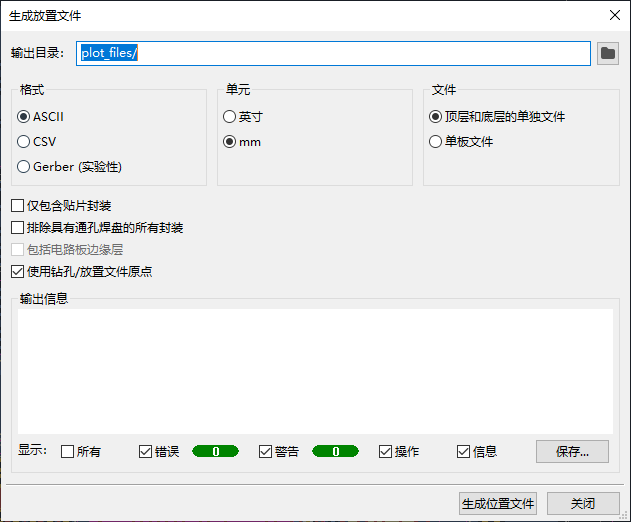
Format: Choose between generating a plain text (ASCII), comma-separated text (CSV), or Gerber X3 placement file format.
单位: 在拾放文件中选择元件位置的单位。
文件: 选择是为电路板正面和背面的封装生成单独的文件,还是生成一个合并两面的文件。
只包括 SMD 封装: 启用后,将只包括具有 SMD 制造属性的封装。 请与您的制造商联系,以确定是否应将非 SMD 封装纳入或排除在位置文件之外。
排除所有带通孔焊盘的封装: 启用时,如果封装包含任何通孔焊盘,即使其制造类型设置为 SMD,也将从拾放文件中排除。
Exclude all footprints with the Do Not Populate flag set: When enabled, footprints will be excluded from the placement file if they have the Do Not Populate attribute set. Check with your manufacturer to determine if DNP components should be included or excluded from the position file.
包括电路板边缘层: 对于 Gerber 放置文件,控制电路板边框是否包含在封装放置数据中。
使用钻孔/拾放文件原点: 启用后,元件位置将相对于电路板设计中设置的钻孔/拾放文件原点。 禁用时,位置将相对于页面原点 (左上角)。
Use negative X coordinates for footprints on bottom layer: When enabled, the X coordinates will be flipped (negated) for footprints on the bottom layer.
其它制造输出
KiCad 还可以从电路板设计中生成封装报告文件、IPC-D-356 网表文件和物料清单 (BOM)。 这些输出格式没有可配置的选项。
打印
KiCad 可以使用文件菜单中的打印操作将电路板视图打印到标准打印机上。
包含层: 选择要包含在打印输出中的层。未选中的层将不可见。右击列表以获取图层选择命令。
输出模式: 选择以黑白或全彩方式打印。
打印绘图页: 启用后,将打印页面边框和标题块。
根据外观管理器的对象选项卡打印: 如果启用,任何在外观面板的对象选项卡中被隐藏的对象将在打印输出中将被隐藏。 禁用时,如果在包含的图层区域中选择了这些对象所在的图层,则将打印这些对象。
打印背景色: 全彩色打印时,该选项控制是否打印视图背景色。
使用不同的颜色主题进行打印: 当以全色打印时,此选项允许使用不同的颜色主题进行打印。 禁用时,电路板编辑器使用的颜色主题将用于打印。
钻孔标记: 控制是以实际大小显示钻孔,还是以较小的尺寸显示钻孔,或是将其隐藏在打印输出中。
打印镜像: 启用后,打印输出将被水平镜像。
每层打印一页: 启用后,在 “包含图层” 区域中选择的每一图层都将打印到单独一页。 如果启用此选项,在所有页面上打印电路板边框 选项控制是否将 Edge.Cuts 层添加到每个打印页面。
比例: 控制打印输出相对于页面设置中配置的页面大小的比例。
导出文件
KiCad can export a board design to various third-party formats for use with external software. These functions are found in the Export section of the File menu.
Specctra DSN exporter
The Specctra DSN exporter creates a file suitable for importing into certain third-party autorouter software. This exporter has no configurable options.
GenCAD exporter
The GenCAD exporter creates a GenCAD file for fabrication, testing, or importing into other software.
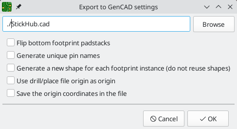
The GenCAD exporter has several options.
Flip bottom footprint padstacks: If enabled, separate flipped padstack definitions will be added for bottom-side footprints. This may be necessary for importing into some third-party software.
Generate unique pin names: If enabled, a suffix will be added to each pin name so that no footprint in the generated file will have two pins with the same name.
Generate a new shape for each footprint instance: If enabled, a unique footprint will be output for every footprint instance, even if two footprints are identical.
Use drill/place file origin as origin: If enabled, coordinates in the generated file will be relative to the drill/place file origin.
Save the origin coordinates in the file: If enabled, the selected origin coordinates will be included in the generated file. If not enabled, the origin in the generated file will be set to (0,0).
VRML exporter
The VRML exporter creates a VRML (.wrl) 3D model file containing the PCB and any VRML files specified in footprints. VRML models are suitable for use in applications where visual appearance is important and dimensional accuracy is not critical.
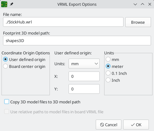
The VRML exporter has several options.
Coordinate origin options: Selects the origin for the generated model. If user defined origin is selected, you can manually specify the origin point.
VRML units for output files: Selects the unit system for the generated model. Dimensions in the generated model will be scaled appropriately.
Copy 3D model files to 3D model path: If enabled, VRML files referenced in footprints will be copied into a subdirectory of the directory containing the generated board VRML model, and the generated model will reference the copied files. The subdirectory name is set by the footprint 3D model path field. If disabled, VRML files referenced in footprints will be embedded in the generated VRML files.
Use relative paths to model files in board VRML file: If enabled, references to external models will use paths relative to the generated board VRML file. If disabled, the references will use absolute paths. This option is only available when the copy 3D model files to 3D model path option is enabled.
IDF exporter
IDF 导出器导出一个 IDFv3 兼容的板(.emn)和库(.emp)文件,用于向机械 CAD 软件传递机械尺寸。导出器导出板子的边框和切口,所有的焊盘和安装孔,包括开槽孔,以及元件的边框;这是与机械设计师互动所需的最基本的机械数据集。IDFv3 规范中描述的所有其他实体目前都没有导出。
| You must attach IDF component models to your design’s footprints before they will be included in the exported model. For more information on attaching models to footprints, see the footprint documentation. Some IDF-specific guidance is included in the Advanced Topics documentation. |
| For more information on creating IDF component models, including descriptions of the IDF utility tools included with KiCad, see the Advanced Topics documentation. |
一旦为所有需要的元件指定了模型,就可以导出电路板的模型。在 PCB 编辑器中,选择文件 → 导出 → IDFv3…。
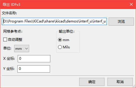
网格参考点: 选择导出的模型参考点的位置。如果选择了 自动调整 选项,KiCad 将把参考点设置为 PCB 的中心点。否则,参考点将相对于显示原点设置。
输出单位: 选择输出模型的单位是毫米还是mil。
输出结果可以直接在机械 CAD 应用程序中查看,或使用 idf2vrml 工具 转换为 VRML。
STEP exporter
The STEP exporter creates a STEP (.step) 3D model file containing the PCB and any STEP files specified in footprints. STEP models are suitable for use in mechanical CAD applications.
The STEP exporter can also export a binary GLTF (.glb) model file by changing the output file’s format to Binary GLTF.
KiCad’s footprint library includes both STEP and VRML (.wrl) versions of each model.
However, footprints in KiCad’s library only reference the VRML versions of the models.
VRML models are not included in STEP exports, but the STEP exporter will instead include
the corresponding STEP version of the model if the subsitute similarly named models
option is enabled.
|
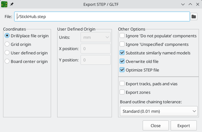
Coordinates: Selects the origin for the generated model. If user defined origin is selected, you can manually specify the origin point.
Ignore 'Do not populate' components: If enabled, components with the DNP attribute set will not be included in the exported STEP model.
Ignore 'Unspecified' components: If enabled, components with the Unspecified footprint type will not be included in the exported STEP model.
Substitute similarly named models: VRML models cannot be used for STEP exports, but if this option is enabled the exporter will look for an identically named STEP model to include in the export instead of a footprint’s specified VRML model. Note that footprints in KiCad’s footprint library specify VRML models, but suitably named STEP models are included for each VRML model. Therefore this option must be enabled in order to export STEP models for footprints from KiCad’s library.
Overwrite old file: If enabled, the exported STEP model will overwrite an existing file with the same name.
Optimize STEP file: If enabled, parametric curves will be disabled in the exported STEP model. This reduces the file size, but may reduce compatibility with some software.
Export tracks, pads and vias: If enabled, tracks, pads, and vias on outer layers will be modeled in the exported STEP model. This option may increase the export time.
Export zones: If enabled, zones on outer layers will be modeled in the exported STEP model. This option may increase the export time.
Board outline chaining tolerance: Controls the minimum distance between two points for the points to be considered coincident. If the board outline in the exported STEP model is not contiguous, try increasing this tolerance.
SVG exporter
The SVG exporter creates a vector graphics image of the board.
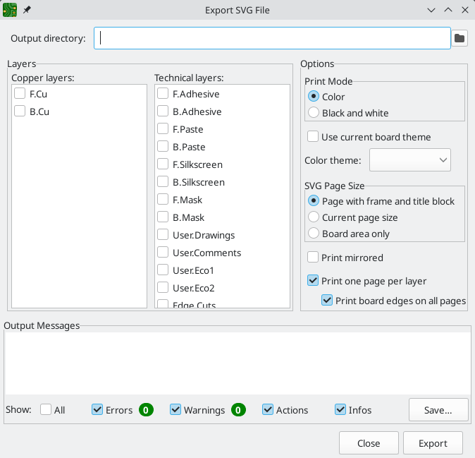
Layers: The selected layers will be included in the generated SVG.
Print mode: Controls whether the generated SVG file is in color or black and white.
Color theme: Controls the color theme used for the generated SVG file. If the use current board theme option is selected, the theme that is selected in the board editor will be used.
SVG page size: Controls the size of the generated SVG drawing. If page with frame and title block is selected, the drawing will match the board’s sheet size and will include the drawing sheet and title block. If current page size is selected, the drawing will match the board’s sheet size but will not include the drawing sheet. If board area only is selected, the drawing will be just big enough to fit the board itself.
Print mirrored: When selected, layers will be horizontally mirrored.
Print one page per layer: When selected, a separate SVG file will be generated for each
selected layer. If the print board edges on all pages option is selected, the Edge.Cuts
layer will be included in all generated SVGs, even if it is not selected as a layer.
Footprint association (CMP) exporter
CMP files are used to sync footprint assignments and some other footprint fields between the PCB and the schematic. You can import CMP files into the schematic using the schematic editor’s File → Import → Footprint Assignments menu item. This provides a very limited form of back annotation. It is recommended to use the Update Schematic from PCB tool instead.
This exporter has no configurable options.
Hyperlynx exporter
The Hyperlynx exporter creates a file suitable for importing into Mentor Graphics (Siemens) HyperLynx simulation and analysis software. This exporter has no configurable options.
封装和封装库
KiCad organizes footprints into footprint libraries, which hold collections of footprints. Each footprint in a board is uniquely identified by a full name that is composed of a library nickname and a footprint name. For example, the identifier Capacitor_SMD:C_0603_1608Metric refers to the C_0603_1608Metric footprint in the Capacitor_SMD library.
管理封装库
KiCad 使用一个封装库表,将所有支持的库类型的封装库映射到库的昵称(Nickname)。KiCad 使用一个全局封装库表,以及一个针对每个工程的表。要编辑任何一个封装库表,请使用 偏好设置→ 管理封装库…。
全局封装库表包含了始终可以使用的库列表,无论当前加载的工程是什么。该表保存在 KiCad 配置文件夹中的 fp-lib-table 文件中。该文件夹的位置 取决于正在使用的操作系统。
工程专用的封装库表包含了专门为当前加载的工程提供的库的列表。如果有任何工程专用的封装库,该表将保存在工程文件夹中的 fp-lib-table 文件中。
KiCad’s footprint library management system allows directly using many types of footprint libraries, including formats that are native to other non-KiCad EDA tools:
-
KiCad
.prettyfootprint libraries (folders with.prettyextension, containing.kicad_modfiles) -
KiCad Legacy footprint libraries (
.modfiles) -
Altium Designer (
.PcbLibor.IntLibfiles) -
CADSTAR PCB Archive (
.cpafiles) -
Eagle footprint libraries (
.lbrfiles) -
EasyEDA / JLCEDA Standard Edition (
.jsonor.zipfiles) -
EasyEDA / JLCEDA Professional Edition (
.elibz,.epro, or.zipfiles) -
GEDA libraries (folders containing
.fpfiles)
Non-KiCad footprint libraries, including KiCad Legacy footprint libraries, can be migrated to KiCad .pretty format using the Migrate Libraries button (see the migrating libraries section).
KiCad only supports writing to KiCad’s native .pretty format footprint libraries (and the .kicad_mod footprint files within them). All other footprint library formats are read-only. To modify a non-KiCad format footprint library, you must first convert it to KiCad format.
|
初始配置
当 PCB 编辑器(或任何其他使用封装的 KiCad 工具)第一次运行时,如果没有找到全局封装表文件 fp-lib-table,KiCad 将引导用户设置一个新的封装库表。该过程在 上文 中描述。
管理表的条目
封装库只有在被添加到全局或工程专用的封装库表中时才能被使用。
通过点击 ![]() 按钮并选择一个库或点击
按钮并选择一个库或点击 ![]() 按钮并输入库文件的路径来添加一个库。选定的库将被添加到当前打开的库表中(全局或工程专用)。可以通过选择所需的库条目并点击
按钮并输入库文件的路径来添加一个库。选定的库将被添加到当前打开的库表中(全局或工程专用)。可以通过选择所需的库条目并点击 ![]() 按钮来删除库。
按钮来删除库。
点击 ![]() 和
和![]() 按钮在库表中上下移动所选库。这并不影响在 "封装库浏览器"、"封装编辑器 "或 "添加封装工具 "中显示库的顺序。
按钮在库表中上下移动所选库。这并不影响在 "封装库浏览器"、"封装编辑器 "或 "添加封装工具 "中显示库的顺序。
通过取消选中第一列中的 活动 复选框,可以使库处于非活动状态。 非活动库仍在库表中,但不会出现在任何库浏览器中,也不会从磁盘加载,这样可以减少加载时间。
点击范围内的第一个库,然后 Shift 点击范围内的最后一个库,可以选择一系列库。
每个库必须有一个独特的昵称:在同一个表中不允许有重复的库昵称。然而,昵称可以在全局和工程库表中重复。工程表中的库比全局表中的同名库更有优先权。
库的昵称不一定要与库的文件名或路径有关。冒号字符 (:) 不能用于库昵称或封装名称,因为它被用作昵称和封装之间的分隔符。
Each library entry must have a valid path. Paths can be defined as absolute, relative, or by path variable substitution.
The appropriate library format must be selected in order for the library to be properly read. The supported formats are listed above. Only KiCad format libraries (.pretty folders containing .kicad_mod files) can be saved. Other footprint library formats are read-only and must be converted to KiCad format before you can modify them.
有一个可选的描述字段,用于添加库条目的描述。选项字段目前不使用,所以添加选项在加载库时不会有任何影响。
Path Variable Substitution
The footprint library tables support path variable substitution, which allows you to define path variables containing custom paths to where your libraries are stored. PATH variable substitution is supported by using the syntax ${PATH_VAR_NAME} in the footprint library path.
By default, KiCad defines several path variables which are described in the project manager documentation. Path variables can be configured in the Preferences → Configure Paths… dialog.
Using path variables in the footprint library tables allows libraries to be relocated without breaking the footprint library tables, so long as the path variables are updated when the library location changes.
${KIPRJMOD} is a special path variable that always expands to the absolute path of the current project directory. ${KIPRJMOD} allows libraries to be stored in the project folder without having to use an absolute path in the project library table. This makes it possible to relocate projects without breaking their project library tables.
使用 GitHub 插件
| KiCad 在 6.0 版本中取消了对 GitHub 库插件的支持。 |
Migrating footprint libraries to KiCad format
Non-KiCad format libraries, including legacy libraries (.mod files), are read-only. They need to be converted to KiCad format (.kicad_mod files in a .pretty folder) before you can save changes to them.
| As with most KiCad files, newer versions of KiCad can open older-format library files, but older versions of KiCad cannot read files once they have been saved by a newer version of KiCad. |
Libraries in other formats can be converted to KiCad libraries by selecting them in the footprint library table and clicking the Migrate Libraries button. Multiple libraries can be selected and migrated at once by Ctrl-clicking or shift-clicking.
Libraries can also be converted one at a time by opening them in the Footprint Editor and saving them as a new library.
创建和编辑封装
A footprint is the physical interface between a component package and a circuit board. Footprints can contain:
-
Pads, which define how the component will be physically assembled onto the footprint. When a footprint is added to a board, tracks are routed to pads, and pads provide a magnetic snapping point for the router to connect the pad to a track. Pad shapes and layers are fully customizable, and pads can have plated holes, unplated holes, or no hole.
-
Graphic shapes and text for technical or aesthetic purposes. Graphics can be placed on physical layers (e.g. silkscreen or soldermask) or nonphysical layers. Graphic shapes can also be placed on copper layers, in which case they can make electrical connections.
-
3D models for mechanical CAD and visualization. 3D models are external files that footprints can link to; they are not embedded in footprints.
-
Metadata associated with the footprint.
Footprints in KiCad are organized into footprint libraries, which contain zero or more footprints. Generally footprints are logically grouped by footprint category, function, and/or manufacturer. Each library is a folder (usually ending in .pretty) containing a .kicad_mod file for each footprint in the library.
Footprint editor overview
KiCad provides a footprint editing tool that allows you to create footprint libraries; add, edit, delete, or transfer footprints between libraries; export footprints to files; and import footprints from files. The Footprint Editor can be launched from the KiCad Project Manager or from the Board Editor (Tools → Footprint Editor).
The Footprint Editor main window is shown below. It has three toolbars for quick access to common features and a footprint viewing/editing canvas. Not all commands are available on the toolbars, but all commands are available in the menus.
In addition to the toolbars, there are collapsible panels for the footprint tree and properties manager (not shown) on the left, and the appearance panel and selection filter on the right. The bottom of the window contains a message panel that shows details about the selected object.
Top toolbar
The main toolbar is at the top of the main window. It has buttons for the undo/redo commands, zoom commands, footprint/pad properties dialogs, and layer/grid management controls.
|
Create a new footprint in the selected library. |
|
Create a new footprint in the selected library using a footprint wizard. |
|
Save the currently selected footprint. |
|
Print the currently selected footprint. |
|
Undo last edit. |
|
Redo last undo. |
|
Refresh display. |
|
Zoom in. |
|
Zoom out. |
|
Zoom to fit footprint in display. |
|
Zoom to fit selection. |
|
Rotate selected item(s) counter-clockwise. |
|
Rotate selected item(s) clockwise. |
|
Mirror selected item(s) horizontally. |
|
Mirror selected item(s) vertically. |
|
Add the selected item(s) to a group. |
|
Remove the selected item(s) from a group. |
|
Edit the current footprint’s properties. |
|
Edit the selected pad’s properties. |
|
Test the current footprint for design errors. |
|
Edit a footprint in the current board in the footprint editor. |
|
Insert current footprint into the board. |
左侧工具栏显示控件
The left toolbar provides options to change the display of items in the Footprint Editor.
|
Turn grid display on/off. Note: by default, hiding the grid does not disable grid snapping. This behavior can be changed in the Display Options section of Preferences. |
|
Turn item-specific grid overrides on/off. |
|
Switch between polar and Cartesian coordinate display in the status bar. |
|
Display/entry of coordinates and dimensions in inches, mils, or millimeters. |
|
Switch between full-screen and small editing cursor (crosshairs). |
|
Switch between free angle and 45 degree mode for placement of new tracks, zones, graphical shapes, dimensions, and other objects. You can also toggle between free angle and 45 degree mode using Shift+Space. |
|
Switch display of pads between filled and outline mode. |
|
Switch display of graphic items between filled and outline mode. |
|
Switch display of text between filled and outline mode. |
|
Switch the non-active layer display mode between Normal and Dim. Note: this button will be highlighted when the non-active layer display mode is either Dim or Hide. In both cases, pressing the button will change the layer display mode to Normal. The Hide mode can only be accessed via the controls in the Appearance Panel or via the hotkey Ctrl+H. |
|
Toggle display of library and footprint tree. |
|
Show or hide the Appearance and Selection Filter panels on the right side of the editor. |
|
Show or hide the Properties Manager panel on the left side of the editor. |
Right toolbar tools
Placement and drawing tools are located in the right toolbar.
|
Selection tool (the default tool). |
|
Pad placement tool: click on the board to place a pad. |
|
Add rule area: Rule areas, formerly known as keepouts, can restrict the placement of items and the filling of zones and can also define named areas to apply specific custom design rules to. |
|
Draw lines. Note: Lines are graphical objects and are not the same as tracks placed with the Route Tracks tool. Graphical objects cannot be assigned to a net. |
|
Draw arcs: pick the center point of the arc, then the start and end points. By right clicking this button, you can change the arc editing mode between a mode that maintains the existing arc center and a mode that maintains the arc radius. |
|
Draw rectangles. Rectangles can be filled or outlines. |
|
Draw circles. Circles can be filled or outlines. |
|
Draw graphical polygons. Polygons can be filled or outlined. Note: Filled graphical polygons are not the same as filled zones: graphical polygons cannot be assigned to a net and will not keep clearance from other items. |
|
Add bitmap image for reference. Reference images are not included in fabrication outputs. |
|
Add text. |
|
Add a textbox. |
|
Add dimensions. Dimension types are described in more detail below. |
|
Deletion tool: click objects to delete them. |
|
Anchor tool. Left-click to set the anchor position (origin) of the footprint. |
|
Set grid origin. |
|
Interactively measure the distance between two points. |
Browsing, modifying, and saving footprints
The ![]() button displays or hides the list of available libraries, which allows you to select an active library. When a new footprint is created, it will be placed in the active library.
button displays or hides the list of available libraries, which allows you to select an active library. When a new footprint is created, it will be placed in the active library.
Clicking on a footprint name opens that footprint in the editor, and hovering the cursor over the name of a footprint displays a preview of the footprint.
After modification, a footprint can be saved in the current library or a different library. To save the modified footprint in the current library, click the ![]() button.
button.
To save the footprint changes to a new footprint, click File → Save As…. The footprint can be saved in the current library or a different library, and a new name can be set for the footprint.
To create a new file containing only the current footprint, click File → Export → Footprint…. This file will be a standard footprint library which will contain only one footprint.
Creating a new footprint library
You can create a new footprint library by clicking File → New Library…. At this point you must choose whether the new library should be added to the global footprint library table or the project footprint library table. Libraries in the global library table will be available to all projects, while libraries in the project library table will only be available in the current project.
Following selection of the library table, you must choose a name and location for the new library. A new, empty library will be created at the specified location.
Creating a new footprint
To create a new footprint in the current footprint library, click the ![]() button or click File → New Footprint…. You will be prompted for new footprint’s name and its footprint type.
button or click File → New Footprint…. You will be prompted for new footprint’s name and its footprint type.
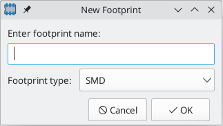
The name will set the name of the footprint, which is used when assigning a footprint to a symbol, and is also used as the filename of the footprint file on disk.
The type can be Through hole, SMD, or Other. Footprint type should be set appropriately, as it has several effects on pad creation, board inspection, DRC, and output generation. The footprint type can be changed after the footprint is created, however.
After clicking OK, a new footprint will be created in the selected library.
The new footprint will be empty except for several default text items. The footprint contains two default (mandatory) footprint fields, Reference and Value. Reference contains the text REF**, which will be replaced with the reference designator of the footprint’s corresponding symbol when the footprint is added to the board. Value initially contains the footprint’s name, but this will also be updated with the contents of the corresponding symbol’s Value field when the footprint is added to the board. Finally, there is a footprint text item containing the string ${REFERENCE}, which is a text variable that will resolve to the value of the footprint’s Reference field once the footprint is on a board.
These items are centered on the footprint’s anchor (origin point), which is indicated with a magenta cross symbol. The anchor can be repositioned (changing the (0, 0) point for the footprint) by selecting the ![]() button and clicking on the new desired anchor position.
button and clicking on the new desired anchor position.
| Rather than manually creating a footprint, for some common footprints you can use a footprint wizard to create a footprint based on a set of parameters. |
Editing footprint properties
Footprints have a number of properties and metadata items that can be defined. These include text fields, attributes that can be set or not (such as Do Not Populate), clearance and zone connection settings, and 3D model paths. These are initially defined in the library copy of the footprint, but they can be modified on a per-instance basis once a footprint is added to a board. In other words, two copies of the same footprint on a single board can their properties edited separately.
Some properties, namely text fields and attributes, will be automatically set for each footprint in a board based on the fields and attributes in the footprint’s corresponding schematic symbol. Fields and attributes are synced from symbols to footprints when you perform the Update PCB From Schematic action. They are also synced from footprints back to symbols when you perform the Update Schematic From PCB action.
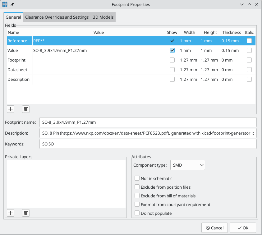
To edit footprint properties, click the ![]() button to show the Footprint Properties dialog. You can also double click an empty spot in the editing canvas.
button to show the Footprint Properties dialog. You can also double click an empty spot in the editing canvas.
Footprint name, description, and keywords
The footprint name, description, and keywords describe the footprint itself. Together they are intended to describe the footprint and help you select an appropriate footprint for each component. They are also used when searching for footprints in the Footprint Editor and the Add Footprint dialog.
The footprint name contains the name of the footprint. This is the same as the footprint’s filename on disk, and is also initially the same as the footprint’s Value field. However, the Value field can be edited in the footprint editor, and when a footprint is added to a board, its Value field will be updated with the value of the footprint’s corresponding symbol.
The description is a description of the footprint. It should be human readable, but it is also used when searching for a footprint.
This description property is specifically a description of the
footprint. This is not to be confused with the Description field,
which will be set to the description of the footprint’s corresponding
symbol when the footprint is added to a board.
|
The keywords are space-separated words related to the footprint. They are used when searching for a footprint.
Footprint fields
Footprints contain multiple fields, which are named values containing information related to the footprint. Fields can be visible and shown on any board layer, or they can be hidden and only shown in the footprint’s properties. Some fields have special meaning to KiCad: Reference and Footprint are both both used by KiCad to identify schematic symbols and PCB footprints, for example. Other fields may contain information that is important for a design but is not interpreted by KiCad, like pricing or stock information for a part.
Any fields defined in a library footprint will be included in the footprint when it is added to a board. You can also add new fields to footprints in the board. Whether they are in the library footprint or not, these fields can then be edited on a per-footprint basis in the board. Symbol fields are also transferred to the board and added as fields in the corresponding footprint.
| Footprint fields are different than graphic text. In addition to being named, fields can be moved and edited in the board, while footprint text can only be edited in the footprint editor. Before KiCad version 8.0, footprints did not have fields, only graphic text, and this graphic text could be edited directly in the board editor. |
All library footprints are defined with five default fields which correspond to the five default fields in library symbols: Reference, Value, Footprint, Datasheet, and Description. These default fields cannot be deleted. The Reference field initially has the value REF**, while the Footprint and Value fields are initially set to the name of the footprint. In the board, the values of the five default fields will be set to the values of the matching fields in the footprint’s corresponding symbol.
The Description footprint field is the description of the symbol, not
the footprint, and will be overwritten by the value of the corresponding
symbol’s description. Footprints have a separate footprint description
property (not a field), which is specifically intended for a description
of the footprint.
|
Fields each have an associated layer, which determines which board layer the field will be placed on. Fields can also be visible or hidden.
To edit an existing footprint field, double-click the field, select it or hover and press E, or right-click on the field text and select Properties….
To add new fields, delete optional fields, or edit existing fields, use the ![]() icon on the main tool bar to open the Footprint Properties dialog. Fields can be arbitrarily named, but names starting with
icon on the main tool bar to open the Footprint Properties dialog. Fields can be arbitrarily named, but names starting with ki_, e.g. ki_description, are reserved by KiCad and should not be used for user fields.
Fields have a number of properties, each of which is shown as a column in the properties grid. Not all columns are shown by default; columns can be shown or hidden by right clicking on the grid header and selecting or deselecting columns from the menu.
封装属性
Footprints have several attributes, which are properties of the footprint that affect how it is handled by other parts of KiCad.
Every footprint has a component type: SMD, Through hole, or Unspecified. A footprint’s type affects KiCad’s behavior in a few ways:
-
Footprint type controls the default type of new pads added to the footprint. For through hole and Unspecified footprints, new pads will be through hole by default, although they can be changed after creation. For SMD footprints, new pads will be SMD by default.
-
Footprint type can be used to filter footprints from component placement files as well as other exports, such as STEP files. Additionally, the footprint type is included as metadata in IPC-2581 exports.
-
Footprint 3D models can be shown and hidden in the 3D viewer based on their type. For example, SMD models can be hidden while through hole models are still displayed.
-
Footprints of different types are reported separately in the Board Statistics dialog.
-
DRC will report footprints containing pads that do not match the parent footprint’s type, for example SMD pads in a through hole footprint.
If not in schematic is checked, KiCad will not expect the footprint to correspond to a symbol in the schematic. When updating a PCB from the schematic, KiCad will ordinarily remove footprints that don’t have corresponding symbols according to the delete footprints with no symbols setting. However, such footprints will not be deleted when they have not in schematic set.
If exclude from POS files is checked, KiCad will not include the footprint in component placement file exports.
If exclude from bill of materials is checked, the component will not be included in bill of materials exports in either the schematic or PCB editors. This attribute is synced to and from the footprint’s corresponding schematic symbol.
If exempt from courtyard requirement is checked, the footprint will not trigger a DRC violation if it does not contain a courtyard. Without this attribute set, a footprint without graphics on the F.Courtyard or B.Courtyard layer will cause a "Footprint has no courtyard defined" DRC violation.
The do not populate attribute is primarily a schematic symbol attribute, and is synced to and from the footprint’s corresponding schematic symbol. Footprints with this attribute set can optionally be excluded from component placement file exports and some other types of outputs. These footprints can also be hidden in the 3D viewer.
Private footprint layers
Footprints can have private footprint layers, which are layers that can be viewed and edited in the Footprint Editor but are not shown in the footprint when it is added to a board. Therefore any objects that are on private layers will not be visible in the PCB Editor or included in PCB fabrication outputs. This may be useful, for example, for notes or graphics that are of interest when drawing or editing a footprint but not needed at the board level.
Any of the existing User.* layers (User.Drawings, User.Comments, User.Eco1, User.1, etc.) can optionally be a private layer. To make a layer private, add a private layer in the General tab of the footprint properties dialog, then select the desired layer. Any objects on that layer will not be shown on the board.
Clearance overrides and settings
The Clearance Overrides and Settings tab holds settings for footprint-specific overrides to board clearance and mask/paste expansion, pad-to-zone connections, and net tie settings for allowing pads within the footprint to short different nets.
Pad clearance controls the minimum clearance between the footprint’s pads and any copper shape
(tracks, vias, pads, zones) on a different net. This value is normally set to 0 which will cause
the pad clearance to be inherited from the board’s design rules and netclass rules. This value can
be overridden for individual pads by setting the pad’s clearance to a nonzero value.
The aperture appearing on any technical layer will have the same shape and size as the pad shape on the copper layer(s). In the PCB manufacturing process, the manufacturer will often change the relative size of mask and paste apertures relative to the copper pad size, but since this size change is specific to a manufacturing process, most manufacturers expect the design data to be provided with the apertures set to the same size as the copper pads. For specific situations where you need to oversize or undersize a technical layer aperture in the design data, you can use the settings here. These values can be overridden for individual pads by setting the pad’s expansion or clearance to a nonzero value.
Solder mask expansion controls the size difference between the pad shape and the aperture shape
on the F.Mask and B.Mask layers. A positive number means the solder mask aperture will be larger
than the copper shape. This number is an inflation applied to all directions. For example, a
value of 0.1mm here will cause the solder mask aperture to be inflated by 0.1mm, meaning that
there will be an 0.1mm border on all sides of the pad and the solder mask opening will be 0.2mm
wider than the pad when measured along a given axis.
Solder paste absolute clearance controls the size difference between the pad shape and the aperture shape on the F.Paste and B.Paste layers. Its behavior is otherwise identical to the behavior of the solder mask expansion setting.
锡膏相对间隙 允许将锡膏间隙值设置为焊盘尺寸的百分比,而不是绝对距离值。 如果同时指定了相对间隙和绝对间隙,它们将被加在一起以确定锡膏孔径的大小。
Pad connection to zones controls whether the footprint’s pads will have solid, thermal relief, or no connection to zones. Like the other overrides, this one may be set for an individual pad or for an entire footprint. The default setting for this control is From zone setting, which uses the connection mode specified in the connection zones' properties. This setting can be overridden for individual pads by setting the pad’s connection mode to a value other than From parent footprint.
Creating net ties
Footprints can act as net ties, where two separate nets are electrically connected by copper. Connecting nets together would normally causes a DRC error due to violating the clearance between two nets, but a footprint can be configured to short nets without causing a DRC violation. This can be used to connect multiple grounds at a specific location, to make kelvin sense connections to a component, or for other applications.
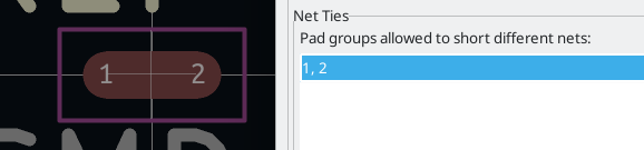
Net ties connect two or more nets in one contiguous region of copper. Each net in a net tie must have its own pad. Pads are not ordinarily allowed to short to other pads; to allow pads to be shorted in net ties, the shorting pads must be added to a net tie group. To create a net tie group, add the pad numbers of the shorting pads to the Net Ties table in the Clearance Overrides and Settings tab of the Footprint Properties dialog. For example, to allow pads 1 and 2 to short in a footprint, add a line to the table with the contents 1,2.
After creating a net tie group, the specified pads are allowed to be electrically shorted. Pads in net tie groups can be connected either by directly overlapping the pads or by adding a copper shape that overlaps both pads.
Footprints can contain multiple net tie groups. Each group can short two or more nets, but every group must remain electrically separate from other groups.
3D models
The 3D Models tab allows you to attach external 3D model files to a footprint and view the footprint in three dimensions along with any attached models.
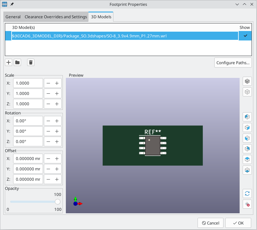
The main part of the window is a 3D preview of the footprint and any attached models. The buttons to the right of the preview let you enable or disable an orthographic projection (![]() ), show or hide the PCB model (
), show or hide the PCB model (![]() ), align the view to one of the six face-aligned perspectives (
), align the view to one of the six face-aligned perspectives (![]() ), and refresh the view (
), and refresh the view (![]() ). The bottom button (
). The bottom button (![]() ) lets you set the thickness of the PCB in the preview.
) lets you set the thickness of the PCB in the preview.
The top of the dialog lets you attach external models. Each added model will be shown in the footprint preview as well as in the full PCB 3D view when the footprint is added to a board. Footprint models can be in STEP, VRML, or IDF format. The models are specified as paths to the model files, which can contain path variables such as ${KIPRJMOD} or ${KICAD8_3DMODEL_DIR}. Click the Configure Paths button to configure path variables. If there is a problem loading a model file from the specified path, an icon in the leftmost column will indicate an error.
KiCad will automatically resolve versioned path variables from
older versions of KiCad to the value of the corresponding variable from
the current KiCad version, as long as the old variable is not explicitly
defined itself. For example, ${KICAD7_FOOTPRINT_DIR} will
automatically resolve to the value of ${KICAD8_FOOTPRINT_DIR} if there
is no KICAD7_FOOTPRINT_DIR variable defined.
|
| Many footprints in KiCad’s standard library do not yet have model files created for them. However, these footprints may contain a path to a 3D model that does not yet exist, in anticipation of the 3D model being created in the future. |
By default, models are added with their origin placed at the footprint’s origin, with no offset, scaling, or rotation. Offset, scaling, and rotation can be applied to a model using the controls to the left of the preview canvas. The model’s opacity can be adjusted using the opacity slider, and the model can be completely hidden by deselecting the show checkbox in the rightmost column of the model table.
Footprint pads
Pads are added to a footprint by clicking the ![]() button in the right toolbar, then clicking again in the desired location in the canvas. The tool will continue adding new pads each time you click on the canvas until you cancel the tool (Esc).
button in the right toolbar, then clicking again in the desired location in the canvas. The tool will continue adding new pads each time you click on the canvas until you cancel the tool (Esc).
New pads in SMD footprints are SMD by default, while new pads in Through Hole and Unspecified footprints will be through hole. Each new pad will have its pad number incremented by 1 relative to the previous pad number.
Pad properties
You can edit a pad after adding it by opening the pad’s properties dialog (E). These properties are also editable using the properties manager.
General tab
The General tab of the pad properties dialog shows the physical properties of the pad, including its geometry, shape, and layer settings.
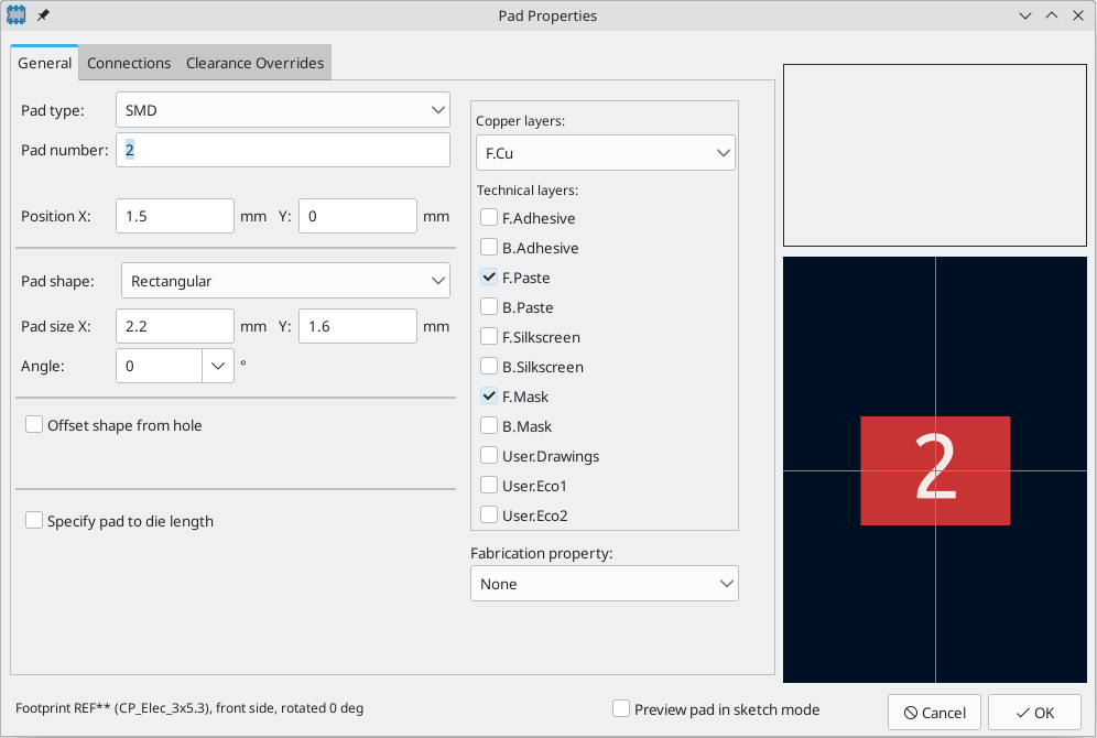
焊盘类型: 此设置控制焊盘的哪些功能被启用。
SMD 焊盘是有电气连接的,没有孔。 换句话说,它们存在于一个单一的铜层上。
通孔 焊盘是有电气连接的,有一个电镀孔。 孔存在于每一层,而铜焊盘存在于多层(见下文 铜层 设置)。
Edge Connector pads are SMD pads that are allowed to overlap the board outline on the
Edge.Cuts layer.
NPTH,机械 焊盘是没有电镀的通孔,不具有电气连接。
SMD 孔洞(钢网印刷版上的孔洞) 焊盘是没有孔和没有电连接的焊盘。 这些可用于在技术层上添加特定的设计,例如锡膏或阻焊孔洞。
铜层 设置控制哪些铜层将有一个与焊盘相关的形状。
For SMD pads, the options are F.Cu or B.Cu, controlling whether the pad sits on the front or the back of the board relative to the footprint’s location. In other words, if a pad is set to exist on B.Cu in its properties, and the footprint is flipped to the back of the board, that pad will now exist on F.Cu, because it also has been flipped.
For through-hole pads, it is possible to remove the pad shape from copper layers where the pad is not electrically connected to other copper (tracks or filled zones). Setting the copper layers to connected layers only will remove the pad shape from any unconnected layers, and setting to F.Cu, B.Cu, and connected layers will remove the pad shape from any internal unconnected layers. This can be useful in dense board designs to increase the routable area on internal layers.
技术层 复选框控制哪些技术层会有一个与焊盘形状相同的孔径。 默认情况下,焊盘在锡膏层和阻焊层上的孔径与铜层相匹配。
| 在当前版本的 KiCad 中,不支持在不同的铜层上定义不同的焊盘形状或尺寸。 |
The Pad number controls what the pad will be electrically connected to in the board. A pad has the same net connection as the pin with the same number in the corresponding schematic symbol.
Pad Position X and Y are the location of the center of the pad, relative to the footprint’s origin.
Pad shape controls the basic shape of the pad. This can be circular, oval, rectangular, trapezoidal, rounded rectangle, chamfered rectangle, chamfered with other corners rounded, custom (circular base), or custom (rectangular base). Each pad shape has its own set of options; for example, rounded rectangles have settings for pad size X and Y, angle, corner size, and corner radius.
| The size of a pad can also be adjusted interactively in the canvas by dragging the editing handles at the pad corners. |
Through-hole and NPTH pads have a hole in addition to the pad itself. The hole shape can be circular or oval, with corresponding size controls. By default the pad is centered on the hole, but the pad can be offset relative to the hole if the offset shape from hole option is enabled (circular pads cannot be offset from the hole).
Fabrication properties are primarily used as metadata in Gerber X2 fabrication output, where the fabrication property is included as an aperture attribute for each pad. The following fabrication properties are available:
BGA pad can only be applied to SMD pads, and only affects Gerber X2 output.
Fiducial, local to footprint and fiducial, global to board only affect Gerber X2 output.
Test point can only be applied to SMD or through hole pads, can only be applied to pads on outer layers, and only affects Gerber X2 output.
Pads with the heatsink pad property are always flashed on every copper layer and are allowed in SMD footprints (PTH pads without this property are not allowed in SMD footprints). It also affects Gerber X2 output.
Pads with the castellated pad* property are allowed to intersect the board edge and still be routed (it is otherwise a DRC error for a pad to intersect the board edge, which makes routing impossible). It also affects Gerber X2 output.
None is for pads for which none of the other fabrication properties apply. It has no effect.
指定焊盘到芯片晶圆(die)的长度: 此设置允许将一个长度与此焊盘相关联,该长度将被布线长度调整工具和网络检测器添加到布线的总长度中。这可以用来指定内部键合线的长度,以便更准确地进行长度匹配,或者在其他某些情况下,网络的电气长度大于电路板上的布线的长度。
Connections tab
The Connections tab contains settings for how pads connect to other objects, including settings for teardrops, zone connections, and thermal reliefs.
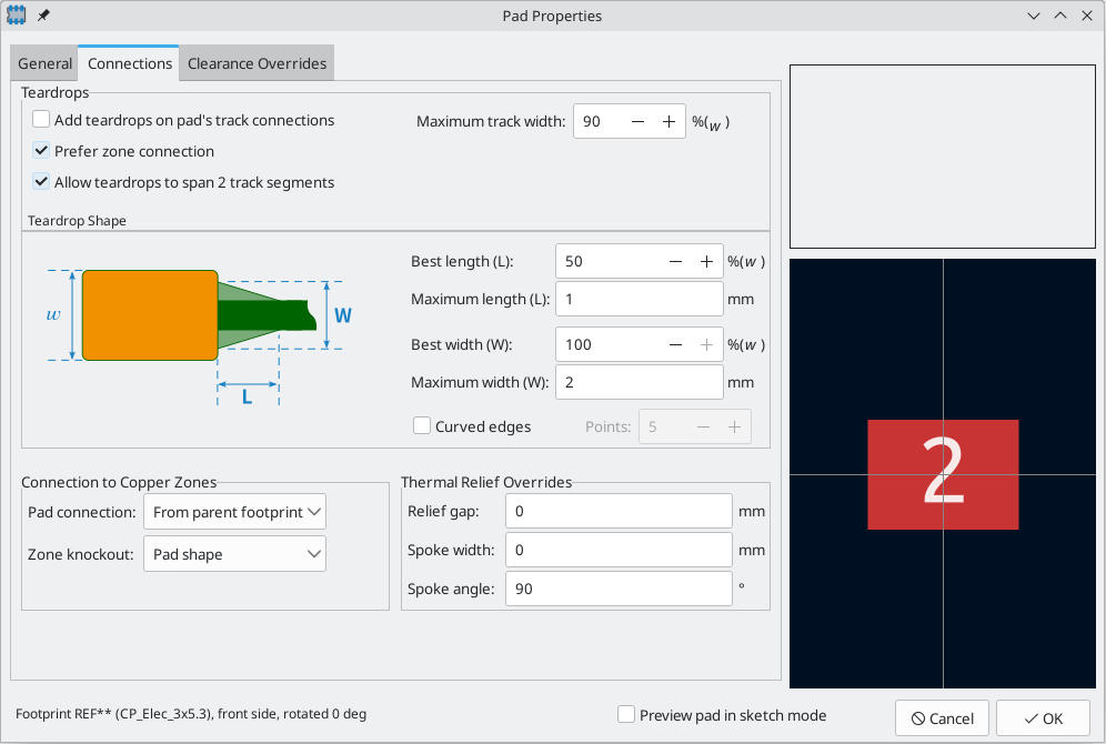
The Teardrops section contains settings controlling teardrop connections between tracks and the pad, if teardrops are used. Teardrop settings are explained in the teardrop documentation.
Pad connection controls whether the pad will have a solid, thermal relief, or no connection to the zone. Like the other overrides, this one may be set for an individual pad or for an entire footprint. The default setting for this control is From parent footprint, and the default footprint setting is to use the connection mode specified in the zone properties.
Zone knockout controls the behavior of the zone filler when the pad uses a custom shape rather than one of the default shapes. This can be used to achieve different results when using thermal reliefs and custom pad shapes.
Relief gap controls the length of the thermal spokes, or the gap between the pad’s shape and
the filled copper area of the zone. This value is normally set to 0 which will cause the relief
gap to be inherited from the connecting zone’s settings.
Spoke width controls the width of the spokes generated when the zone connection mode is
Thermal Relief. This value is normally set to 0 which will cause the spoke width to be
inherited from the connecting zone’s settings.
Clearance Overrides tab
The Clearance Overrides tab holds settings for pad-specific overrides to board clearance and mask/paste expansion.
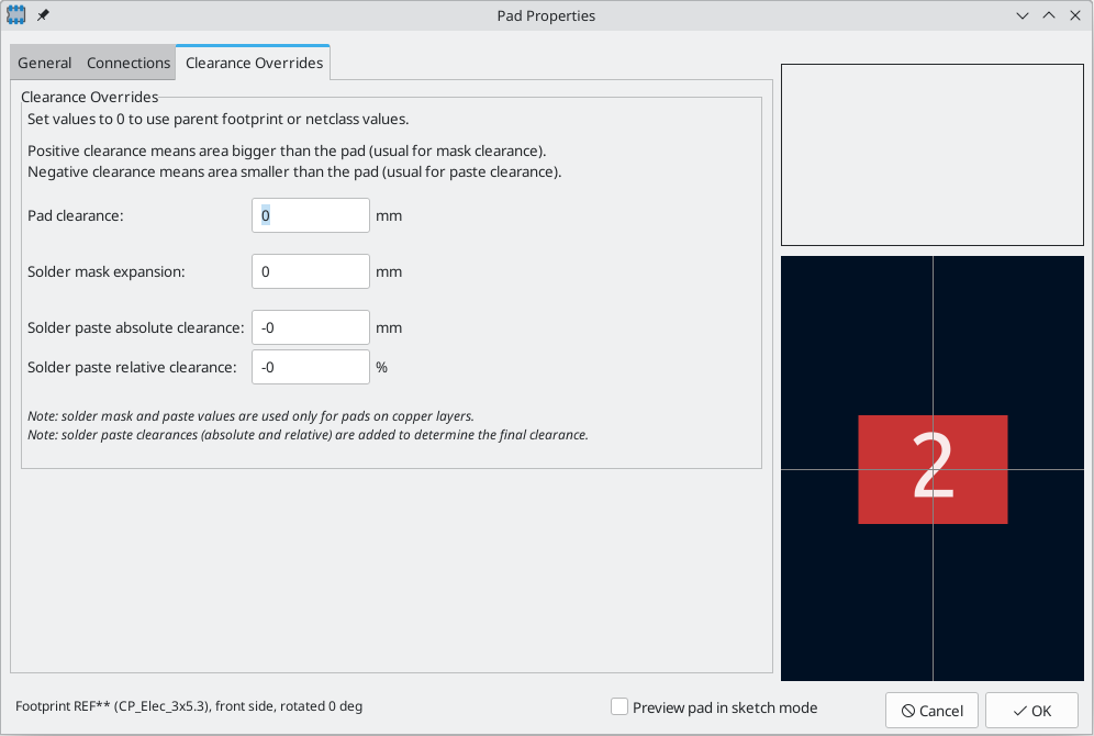
焊盘间隙 控制焊盘与不同网络上的任何铜形状(布线、通孔、焊盘、敷铜)之间的最小间隙。 这个值通常被设置为 0,这将使得焊盘的间隙继承自封装上设置的间隙覆盖或者电路板的设计规则和网络类规则(如果封装的间隙也被设置为 0)。
The aperture appearing on any technical layer will have the same shape and size as the pad shape on the copper layer(s). In the PCB manufacturing process, the manufacturer will often change the relative size of mask and paste apertures relative to the copper pad size, but since this size change is specific to a manufacturing process, most manufacturers expect the design data to be provided with the apertures set to the same size as the copper pads. For specific situations where you need to oversize or undersize a technical layer aperture in the design data, you can use the settings here.
Solder mask expansion controls the size difference between the pad shape and the aperture shape
on the F.Mask and B.Mask layers. A positive number means the solder mask aperture will be larger
than the copper shape. This number is an inflation applied to all directions. For example, a
value of 0.1mm here will cause the solder mask aperture to be inflated by 0.1mm, meaning that
there will be an 0.1mm border on all sides of the pad and the solder mask opening will be 0.2mm
wider than the pad when measured along a given axis.
Solder paste absolute clearance controls the size difference between the pad shape and the aperture shape on the F.Paste and B.Paste layers. Its behavior is otherwise identical to the behavior of the solder mask expansion setting.
锡膏相对间隙 允许将锡膏间隙值设置为焊盘尺寸的百分比,而不是绝对距离值。 如果同时指定了相对间隙和绝对间隙,它们将被加在一起以确定锡膏孔径的大小。
Working with multiple pads
When you place a new pad, the new pad’s properties are copied from the default pad properties. Each time any pad is edited, the pad’s updated properties are stored as the default pad properties, so that new pads will match the properties of the most recently edited pad.
You can directly edit the default pad properties by selecting Edit → Default Pad Properties…, or choose an existing pad to represent the default by right clicking the pad and choosing Copy Pad Properties to Default. New pads will use that pad’s properties as their defaults until a new default is selected, either by editing another pad, editing the default pad properties, or manually copying a different pad’s properties to the default.
There are several ways to update existing pads with the properties of other pads. You can apply the default pad properties to an explicit selection of pads by selecting the desired target pads, right clicking, and choosing Paste Default Pad Properties to Selected from the right click context menu. You can also update other pads with a selected pad’s properties using Push Default Pad Properties to Other Pads…, also in the right click context menu.
This tool has several options to filter which pads are targeted.
If do not modify pads having a different shape is selected, only pads with the exact same shape properties as the selected pad will be updated.
If do not modify pads having different layers is selected, only pads on the same layer(s) as the selected pad will be updated.
If do not modify pads having a different orientation is selected, only pads with the same orientation as the selected pad will be updated.
If do not modify pads pads having a different type is selected, only pads with the same pad type as the selected pad will be updated.
If no options are selected, all pads in the footprint will be updated.
You can create an array of pads from a source pad by right clicking the source pad and selecting Create from Selection → Create Array… (Ctrl+T). The basic functionality of this tool is described in the PCB Editor documentation. For pads, however, there are additional options for controlling pad numbering.
For grid arrays, you can select a numbering direction, either horizontal, then vertical or vertical, then horizontal. If reverse numbering on alternate rows/columns is selected, the direction of increasing pad numbers will alternate from one row/column to the next.
The initial pad number in the array can either be the first unused pad number in the footprint (use first free number) or the specified pad numbering start value. After the first number, the pad numbering can either be continuous (1, 2, 3, …) or coordinate based, in other words, dependent on both the row and column (A1, A2, …, B1, …). In addition to the initial pad number (pad numbering start), you can specify a numbering step (pad numbering skip). For coordinate-based numbering, you can configure separate starting numbers and steps for each axis. You can select whether pad numbers use decimal digits (0-9), hexadecimal digits (0-F), the full alphabet, or the alphabet excepting certain ambiguous letters (I, O, S, Q, X, and Z).
Finally, you can quickly renumber existing pads using the Renumber Pads tool (Edit → Renumber Pads…).
The tool has several options. Pads will be renumbered starting at the selected first pad number, and each subsequent pad will have its number incremented by the numbering step. You can also choose an optional pad name prefix which will be inserted before of the incrementing part of each pad number.
Once you click OK, you will be prompted to click on a pad, which will be assigned a new pad number based on the selected initial pad number and prefix. You can keep clicking on pads to assign them the next number in the sequence based on the selected numbering step. Double click on a pad to renumber that pad and end the sequence, or press Esc to discard the changes.
自定义焊盘形状
For some footprints, the built-in pad shapes (round, rectangular, etc.) may not be sufficient. In these cases you can construct custom pads with arbitrary shapes using Pad Edit Mode. This mode lets you combine a basic pad with graphic shapes to build a new pad out of the compound shape.
To build a custom pad, first add a regular pad using the pad tool (![]() button). This base pad will become the custom pad’s anchor or snapping point, so be sure to place the pad in the exact location where you want tracks to attach to the pad. The shape and size of the pad do not matter, but the hole, if any, will remain in the final custom pad. In other words, a surface mount base pad will result in a surface mount custom pad, and a through hole base pad will result in a through hole custom pad. The custom pad’s number will be inherited from the base pad.
button). This base pad will become the custom pad’s anchor or snapping point, so be sure to place the pad in the exact location where you want tracks to attach to the pad. The shape and size of the pad do not matter, but the hole, if any, will remain in the final custom pad. In other words, a surface mount base pad will result in a surface mount custom pad, and a through hole base pad will result in a through hole custom pad. The custom pad’s number will be inherited from the base pad.
Next, enter Pad Edit Mode by selecting the base pad, right-clicking, and selecting Edit Pad as Graphic Shapes (Ctrl+E). Add graphic shapes as appropriate to create the desired pad shape. Shapes touching the base pad will be unioned together with the base pad to create the final pad shape.
You can exit Pad Edit Mode by right-clicking and selecting Finish Pad Edit, or pressing Ctrl+E again. When you exit pad edit mode, all shapes that touch the base pad will be combined with the pad. For example, when editing a surface mount pad on F.Cu, any shapes that are on F.Cu and touch the base pad will become part of the custom pad. Any shapes that do not overlap the base pad, or that are on a different layer, will remain separate. If the base pad is a through hole pad, overlapping shapes on F.Cu will be combined in the custom pad. Because through hole pads have the same pad shape on all copper layers, this shape will become part of the custom pad on all copper layers, not just F.Cu. For convenience, Pad Edit Mode dims the color of other pads and all shapes that are not contiguous with the base pad so that you can see which shapes will be included in the custom pad and which will not.
Custom pads can only contain a single base pad. Any additional pads that touch the base pad or the contiguous graphics, whether they have the same or different pad numbers as the base pad, will remain separate pads after the shapes are combined into the custom pad.
| If you would like to add multiple anchors (snapping points) to a custom pad, you can add additional separate pads on top of the custom pad. Create the custom pad as normal, containing the first snapping point, then add additional pads with the same number and place them overlapping the custom pad in the desired snapping locations. They will remain distinct pads and will not be combined with the custom pad, but they will act as additional pad anchors and will be electrically connected to the custom pad. |
To modify an existing custom pad, select it and enter Pad Edit Mode again. You can then continue to edit the component shapes to adjust the pad shape, or change the position of the base pad to adjust the pad anchor.
KiCad automatically chooses a size and location for showing the pad number over the pad. Particularly for unusually shaped pads, the automatically determined size and location may not be optimal. In these cases, you can manually specify a region in which KiCad should draw the pad number by adding a pad number box primitive. To add a number box, enter Pad Edit Mode and add a rectangular shape. In the properties manager for the rectangle, check the Number Box checkbox. The rectangle will then be shown as a wireframe, and when you exit Pad Edit Mode it will be used to draw the pad number.
In the board, KiCad will automatically add thermal spokes when connecting the pad to a zone. The thermal spoke settings are determined by the pad, footprint, and zone settings, and the thermal spokes by default connect to the pad anchor. You can override the default thermal spoke placement by adding thermal relief templates to the custom pad. To add a thermal relief template, enter Pad Edit Mode and add a line shape. In the properties manager for the line, check the Thermal Relief Template checkbox. In Pad Edit Mode, the line will then be shown as a wireframe, and it will not be shown outside of pad edit mode. If any thermal relief templates are present in the pad, KiCad will not automatically add additional spokes when filling zones; spokes will only be placed where there are thermal relief templates defined in the pad. Thermal relief templates only determine the spoke location: spoke width and relief gap are still defined in the pad, footprint, and/or zone properties, as normal.
Footprint graphics
Footprints can contain graphic shapes, text, and dimensions. These objects can be placed on nonphysical layers, like F.Fab or User.Drawings, or they can be placed on layers that will be part of the manufactured circuit board, such as Edge.Cuts or a silkscreen, soldermask, or copper layer. Objects on copper layers can make electrical connections.
Closed shapes on a footprint’s F.Courtyard and B.Courtyard layers will form the footprint’s front and back courtyard, respectively. A courtyard defines the physical extents of a footprint and limits where footprints are allowed to be placed in relation to other footprints. If a footprint’s courtyard overlaps another footprint’s courtyard, a DRC violation will be generated.
Shapes on a footprint’s Edge.Cuts layer will correspond to board edges on any PCB that includes the footprint. Closed shapes will result in cutouts, while unclosed shapes will result in unclosed edges. Unclosed edges must be closed in the full board design.
The buttons on the right toolbar can be used to create:
-
Lines (
, default hotkey Ctrl+Shift+L) -
Arcs (
, default hotkey Ctrl+Shift+A) -
Rectangles (
) -
Circles (
, default hotkey Ctrl+Shift+C) -
Polygons (
, default hotkey Ctrl+Shift+P) -
Text (
 , default hotkey Ctrl+Shift+T)
 -
Textboxes (
 )
) -
Dimensions (
 ), of which several types are available
| You can customize the default style of newly-created text and shape objects in Preferences → Footprint Editor → Default Values. |
Graphical objects and their properties are described in more detail in the PCB Editor documentation.
Bulk editing footprint text and graphics
Properties of text and graphics can be edited in bulk using the Edit Text and Graphics Properties dialog (Edit → Edit Text & Graphic Properties…).
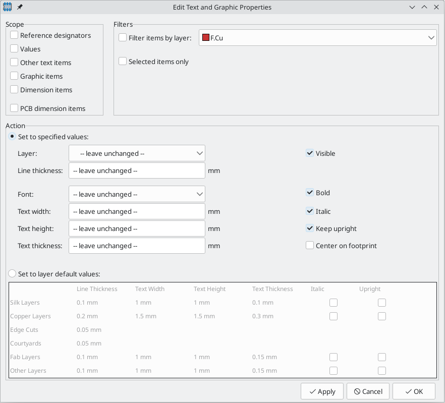
This dialog is described in more detail in the PCB Editor documentation.
Cleaning up footprint graphics
There is a dedicated tool for performing common cleanup operations on graphics, which is run via Tools → Cleanup Graphics….
The following cleanup actions are available and will be performed when selected:
Merge lines into rectangles: combines individual graphic lines that together form a rectangle into a single rectangle shape object.
Delete redundant graphics: deletes graphics objects that are duplicated or degenerate.
Merge overlapping graphics into pads: merges graphic copper shapes that overlap pads into a custom pad.
Any changes that will be applied to the footprint are displayed at the bottom of the dialog. They are not applied until you press the Update Footprint button.
Rule areas
Rule areas, also known as keepouts, are footprint regions that can have specific DRC rules defined for them. Some basic rules are available that will raise DRC errors if certain types of objects are within the bounds of the rule area, but rule areas can also be used together with custom DRC rules to define complex DRC behavior that only applies within the rule area. A rule area in a footprint takes effect when the footprint is added to the board.
You can add a rule area by clicking the ![]() button on the right toolbar (Ctrl+Shift+K). Click on the canvas to place the first corner, which will show the Rule Area Properties dialog. After configuring the rule area appropriately, press OK to continue placing corners of the rule area. The rule area shape can be an arbitrary polygon; click on the starting corner or double click to finish placing the rule area.
button on the right toolbar (Ctrl+Shift+K). Click on the canvas to place the first corner, which will show the Rule Area Properties dialog. After configuring the rule area appropriately, press OK to continue placing corners of the rule area. The rule area shape can be an arbitrary polygon; click on the starting corner or double click to finish placing the rule area.
Rule areas are described in more detail in the PCB editor documentation.
Reference images
Just like in the PCB Editor, you can use reference images in the Footprint Editor to assist with your footprint designs. Footprint reference images are only shown in the Footprint Editor: they are not shown in the PCB Editor when a footprint is added to a board, and they do not appear in any fabrication outputs.
To add a reference image, use the ![]() button on the right toolbar and select the desired reference image file.
button on the right toolbar and select the desired reference image file.
Reference images are described in more detail in the PCB Editor documentation.
封装向导
KiCad provides a set of footprint wizards that can be used to create some common kinds of footprints based on a set of parameters. Wizards for the following types of footprints are provided:
-
BGA packages
-
QFN packages
-
QFP packages
-
SOIC, MSOP, SSOP, TSSOP, etc. packages
-
SIP and DIP packages
-
ZIP packages
-
ZOIC packages
-
FPC connectors
-
Micromatch SMD connectors
-
Circular pad arrays
-
Touch sliders
-
Mutual capacitance touch buttons
-
USS-39 barcodes
-
QR codes
To create a footprint using a footprint wizard, click the ![]() button and choose a footprint type from the list that appears.
button and choose a footprint type from the list that appears.
In the window that appears, fill out the parameters as appropriate. When the parameters are correctly filled out, press the ![]() button to transfer the generated footprint back into the footprint editor. Then you can make additional manual modifications and save the footprint as normal.
button to transfer the generated footprint back into the footprint editor. Then you can make additional manual modifications and save the footprint as normal.
In addition to the set of footprint wizards that KiCad provides, you can also create your own. For more information about creating new footprint wizards, see the Scripting section of the Advanced Topics chapter.
Checking footprints
The Footprint Editor can check for common issues in your footprints. Run the footprint checker using the ![]() button in the top toolbar.
button in the top toolbar.
The footprint checker checks for:
-
Pads that don’t match the footprint’s type: footprints without any through hole pads should be set to the surface mount footprint type
-
Through hole pads without a hole
-
Plated through hole pads not on any copper layers
-
Plated through hole pads without a copper annulus
-
Surface mount pads on both the front and back
-
Surface mount pads with mismatched copper and paste/mask layers (front copper and back paste/mask, or vice versa)
-
Pads that short to other pads outside of net tie groups
-
Nonexistent pads in net tie groups
-
Pads in that appear in multiple net tie groups
Browsing footprint libraries
The Footprint Library Browser allows you to quickly examine the contents of footprint libraries. The Footprint Library Viewer can be accessed by clicking ![]() icon on the main Board Editor toolbar or with View → Footprint Library Browser.
icon on the main Board Editor toolbar or with View → Footprint Library Browser.
To examine the contents of a library, select a library from the list in the left hand pane. All footprints in the selected library will appear in the second pane. Select a footprint name to view the footprint.
Double clicking the name of a footprint or using the ![]() button adds the footprint to the board.
button adds the footprint to the board.
The top toolbar contains the following commands:
|
Select previous footprint in library. |
|
Select next footprint in library. |
|
Zoom tools. |
|
Open footprint in 3D Viewer. |
|
Add the footprint to the board. |
|
Automatically zoom to fit each opened footprint. |
The left toolbar contains the following commands:
|
Selection tool (the default tool). |
|
Interactively measure the distance between two points. |
|
Turn grid display on/off. |
|
Switch between polar and Cartesian coordinate display in the status bar. |
|
Display/entry of coordinates and dimensions in inches, mils, or millimeters. |
|
Switch between full-screen and small editing cursor (crosshairs). |
|
Show or hide pad numbers. |
|
Switch display of pads between filled and outline mode. |
|
Switch display of text between filled and outline mode. |
|
Switch display of graphic items between filled and outline mode. |
高级主题
配置和自定义
KiCad PCB 编辑器有多种偏好设置,可通过偏好设置对话框进行配置。和 KiCad 的所有部分一样,PCB 编辑器的偏好设置存储在用户配置目录中,并且在 KiCad 的小版本之间是独立的,以允许多个版本的偏好设置分别运行。
偏好设置对话框的第一部分(通用、鼠标和触摸板以及快捷键)是所有 KiCad 程序共享的。这些部分在 KiCad 手册中的 "常规偏好设置" 部分有详细描述。
显示选项
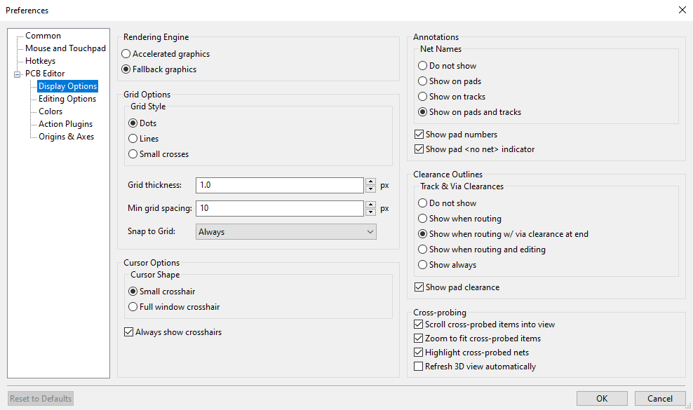
渲染引擎: 控制是否使用硬件加速图形或备用图形加速。
网格样式: 控制对齐网格的绘制方式。
网格粗细: 控制网格线或网格点的粗细。
最小网格间距: 控制两条网格线之间的最小距离 (以像素为单位)。无论当前的网格设置如何,如果网格线 违反这个最小间距,将不会被绘制。
捕捉到网格: 控制绘图和编辑操作何时会被捕捉到活动网格上的坐标。 总是 "将启用捕捉功能,即使网格被隐藏; "当网格显示时" 将只在网格可见时启用捕捉功能。
| 按住 Ctrl 可以暂时禁用网格捕捉。 |
光标形状: 控制编辑光标是画成一个小十字线还是全屏十字线(一组覆盖整个画布的线条)。 编辑光标显示下一个绘图或编辑操作将发生的位置,如果启用了捕捉,则会捕捉到网格位置。
始终显示十字准线: 控制是始终显示编辑光标, 还是仅在编辑或绘图工具处于活动状态时才显示编辑光标。
网络名称: 控制是否在铜对象上绘制网络名称标签。 这些标签仅作为编辑指南,不会出现在制造输出中。
显示焊盘编号:控制是否在封装焊盘上绘制焊盘编号标签。
显示焊盘 <无网络> 指示器: 控制是否用特殊标记指示没有网络的焊盘。
布线间隙: 控制是否显示布线和过孔周围的间隙边界。 间隙边界显示为对象周围的细长形状,表示与其他对象之间的最小间隙, 如约束和设计规则所定义。
显示焊盘间隙: 控制是否显示焊盘周围的间隙边界。
交叉探测项目的中心视图: 当原理图和 PCB 编辑器同时运行时,控制在原理图中点击一个元件或引脚是否会将 PCB 编辑器的视图集中在相应的封装或焊盘上。
缩放以适合交叉探测对象: 控制是否缩放视图以显示交叉探测的 封装或焊盘。
高亮交叉探测网络: 控制当高亮工具在两个工具中激活时,原理图中高亮的网络是否会在 PCB 编辑器中高亮。
编辑选项
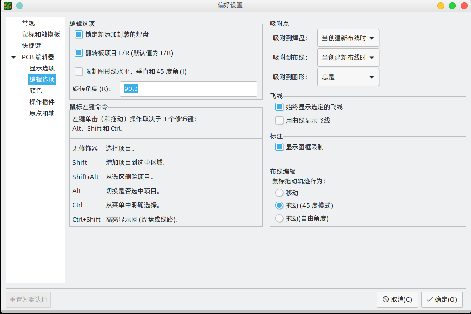
翻转电路板项目 L/R: 控制电路板对象在顶层和底层之间移动时的翻转方向。 选中时,项目从左向右翻转(垂直轴); 取消选中时,项目从上向下翻转(水平轴)。
旋转命令的步长: 控制每次使用旋转命令时选定对象将旋转多远。
允许自由焊盘: 控制封装焊盘是否可以解锁并与封装分开编辑或移动。
吸附点: 这部分控制对象捕捉,也叫吸附点。 启用对象捕捉后,对象捕捉优先于网格捕捉。 对象捕捉只对活动层上的对象起作用。按住 Shift 可以暂时关闭对象捕捉功能。
捕捉焊盘: 控制编辑光标何时捕捉焊盘原点。
捕捉到布线: 控制编辑光标何时捕捉到布线端点。
对齐图形: 控制编辑光标何时对齐图形形状点。
始终显示选定的飞线:启用后,即使全局飞线被隐藏, 选定封装的飞线也将始终显示。
用曲线显示飞线:控制飞线是直线绘制还是曲线绘制。
鼠标拖动布线行为: 控制使用鼠标拖动布线线段时将发生的操作:"移动" 将独立于任何其他布线线段移动布线。 "拖动(45 度模式)" 将调用推挤布线器拖动布线,遵守设计规则并保持其他布线段的连接。 "拖动(自由角度)" 将移动布线段最近的角点,高亮显示与其他对象的碰撞,但不会将其移开。
将操作限制在从起点开始的45度: 控制使用图形绘制工具绘制的布线是否可以采用任何角度。 请注意,这仅影响绘制新的布线:布线可以被编辑成任何角度。
显示页面限制: 控制页面边界是否绘制为矩形。
敷铜属性对话框关闭后重新敷铜: 控制编辑任何敷铜属性后是否自动重新敷铜。 可以在复杂的设计或速度较慢的计算机上禁用此功能,以提高响应速度。
颜色
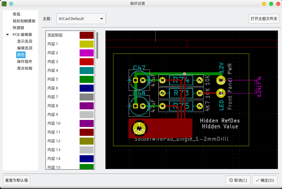
KiCad supports switching between different color themes to match your preferences. Kicad 8.0 comes with two built-in color themes: "KiCad Default" is a new theme designed to have good contrast and balance for most cases and is the default for new installations. "KiCad Classic" is the default theme from KiCad 5.1 and earlier versions. Neither of these built-in themes can be modified, but you can create new themes to customize the look of KiCad as well as install themes made by other users.
颜色主题存储在位于 KiCad 配置目录的 Colors 子目录中的 JSON 文件中。“打开主题文件夹” 按钮将在您的系统文件管理器中打开此位置,使您可以轻松地管理已安装的主题。要安装新主题,请将其放在此文件夹中,然后重新启动 KiCad。如果文件是有效的颜色主题文件,则从颜色主题下拉列表中可以看到新主题。
要创建一个新的颜色主题,从颜色主题的下拉列表中选择 “新主题…”。 为你的主题输入一个名称,然后开始编辑颜色。 新主题中的颜色将从你创建新主题之前选择的任何主题中复制。
要更改颜色,请双击或中键单击列表中的色样。“重置为默认值” 按钮会将该颜色重置为 “KiCad 默认” 颜色主题中的相应条目。
颜色主题会自动保存;当您关闭 "偏好设置" 对话框时,所有更改都会立即反映出来。对话框右侧的窗口显示所选主题外观的预览。
操作插件
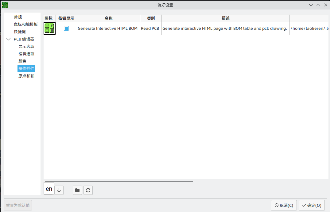
KiCad PCB 编辑器支持用 Python 编写的插件,对正在编辑的电路板进行操作。 这些插件可以使用内置的 “插件和内容管理器” 来安装(详见 KiCad 章节),或者将插件文件放在用户的插件目录中。 详见下面的脚本部分。
每个被检测到的插件都会在这个偏好设置上显示一排。 插件可以在 “PCB 编辑器” 的顶部工具栏上显示一个按钮。 如果一个插件的 "显示按钮" 控制没有被选中,它仍然可以从 "工具" > "外部插件" 菜单中访问。
列表底部的箭头控制允许改变插件在工具栏和菜单中的显示顺序。 文件夹按钮将启动一个文件资源管理器到插件文件夹,以使安装新的插件更容易。 刷新按钮将扫描插件文件夹中的任何新的或删除的插件,并更新列表。
原点和轴
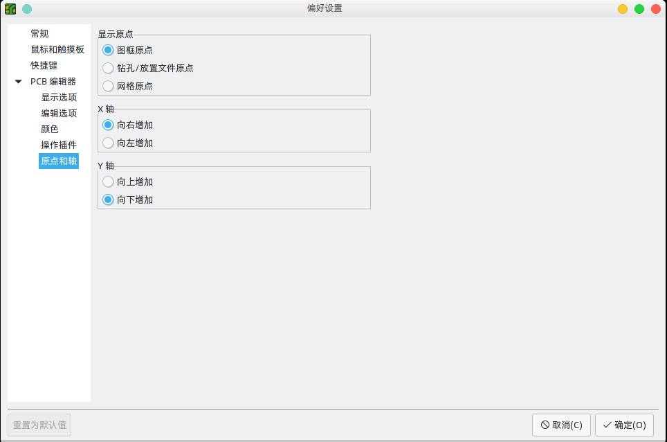
显示原点: 决定在编辑画布中坐标显示使用哪个坐标原点。 页面原点固定在页面的角落。 用户可以移动钻孔/拾放文件原点和网格原点。
X 轴: 控制 X 坐标向右还是向左增加。
Y 轴: 控制 Y 坐标是向上还是向下增加。
文本变量
KiCad支持文本变量,允许你用定义的文本字符串替换变量名称。 这种替换发生在变量名称在 ${VARIABLENAME} 的变量替换语法内的任何地方。
The following variables can be used in PCB text, footprint text, footprint fields, and drawing sheet fields. There are also a number of variables that can be used in the Schematic Editor.
| Variable name | Description |
|---|---|
|
Contents of drawing sheet’s |
|
Contents of drawing sheet’s |
|
Today’s date, in ISO format. |
|
Filename of the board, with a file extension. |
|
Full file path of the board, with a file extension. |
|
Contents of drawing sheet’s |
|
Current version of KiCad. This variable is only available in drawing sheet fields. |
|
Layer of the object. In footprint fields, this is the layer of the parent footprint. In drawing sheet fields, this resolves to the plotted layer. |
|
Current sheet’s paper size. This variable is only available in drawing sheet fields. |
|
Project name, without a file extension. |
|
Contents of drawing sheet’s |
|
Contents of drawing sheet’s |
|
Contents of project text variable
|
|
Contents of footprint field Both built-in footprint fields and user-defined fields from the
corresponding symbol are available. Built-in footprint fields use all
uppercase letters: for example, to access a footprint’s value, use
Built-in footprint fields are |
|
Contents of field Both built-in footprint fields and user-defined fields from the
corresponding symbol are available. Built-in footprint fields use all
uppercase letters: for example, to access the value of Built-in footprint fields are |
自定义设计规则
KiCad 的自定义设计规则系统允许创建比电路板设置对话框的 "约束" 页面中的通用规则更具体的设计规则。 自定义设计规则有很多应用,但一般来说,它们被用来对电路板的一部分应用某些规则,如特定的网络或网络类、特定的区域或特定的封装。
自定义设计规则存储在一个扩展名为 kicad_dra 的单独文件中。当您开始向项目添加自定义规则时,会自动创建此文件。如果您在项目中使用自定义规则,请在备份或提交到版本控制系统时,确保将 kicad_dra 文件与 kicad_pcb 和 kicad_pro 文件一起保存。
kicad_dra 文件由 KiCad 自动管理,不应使用外部文本编辑器进行编辑。
始终使用电路板设置对话框的自定义规则页面编辑自定义设计规则。
|
自定义规则编辑器
自定义规则编辑器位于电路板设置对话框中,它提供了一个用于输入自定义规则的文本编辑器,一个语法检查器将测试你的自定义规则并指出任何错误,还有一个语法帮助对话框,其中包含了对自定义规则语言的快速参考和一些规则示例。
The custom rules editor also provides context-sensitive autocomplete to suggest valid keywords and properties. The autocomplete suggestion menu appears automatically, but it can also be opened manually by pressing Ctrl+Space.
在编辑自定义规则后,最好使用 检查规则语法 按钮,确保没有语法错误。 自定义规则中的任何错误将阻止设计规则检查器的运行。
自定义规则语法
The custom design rule language is based on s-expressions and allows you to create design constraints that are not possible with the built-in constraints. Each design rule generally contains a condition defining what objects to match and a constraint defining the rule to be applied to the matched objects.
该语言使用圆括号 (( 和 )) 来定义相关标记和值的子句。括号必须始终匹配:对于每个 ( 必须有匹配的 )。在子句中,标记和值之间用空格分隔。按照惯例,使用单个空格,但是可以在标记之间使用任意数量的空格字符。在文本字符串有效的地方,没有任何空格的字符串可以用 " 或 ' 引起来,也可以不加引号。包含空格的字符串必须始终用引号引起来。在需要嵌套引号的地方,可以使用 " 作为外引号字符,使用 ' 作为内引号字符 (反之亦然),从而实现单层嵌套。换行符不是必需的,但为清楚起见,通常在示例中使用。
在下面的语法描述中,<三角括号> 中的项目代表必须存在的标记,[方括号] 中的项目代表可选的或只是有时需要的标记。
The Custom Rules file must start with a version header defining the version of the rules language. As of KiCad 8.0, the version is 1. The syntax of the version header is (version <number>). So in KiCad 8.0 the header should read:
(version 1)
在版本头之后,您可以输入任何数量的规则。 规则的评估顺序是相反的,也就是说,文件中的最后一条规则首先被检查。 一旦为一个给定的被测对象找到一个匹配的规则,将不再检查其他规则。在实践中,这意味着更具体的规则应该在文件的后面,以便它们在更通用的规则之前被评估。
例如,如果您创建一条规则来限制 HV 网络的布线与任何其他网络的布线之间的最小间距,然后又创建第二条规则来限制特定规则区域内所有对象的最小间距,请确保第一条规则在自定义规则文件中的出现时间比第二条规则晚,否则,如果 HV 网络中的布线落在规则区域内,可能会有错误的间距。
Each rule must have a name and one or more constraint clauses. The name can be any string and is used to refer to the rule in DRC reports. The constraint defines the behavior of the rule. Rules may also have a condition clause that determines which objects should have the rule applied, an optional layer clause which specifies which board layers the rule applies to, and an optional severity clause which specifies the severity of the resulting DRC violation.
(rule <name>
    [(severity <severity>)]
    [(layer <layer_name>)]
    [(condition <expression>)]
    (constraint <constraint_type> [constraint_arguments]))
The custom rules file may also include comments to describe rules. Comments are denoted by any line that begins with the # character (not including whitespace). You can press Ctrl+/ to comment or uncomment lines automatically.
# Clearance for 400V nets to anything else
(rule HV
    (condition "A.NetClass == 'HV'")
    (constraint clearance (min 1.5mm)))
图层子句
层 (layer) 子句确定规则将对哪些层起作用。虽然对象层可以在下面介绍的 约束 (constraint) 子句中进行测试,但是使用 层 (layer) 子句效率更高。
层 (layer) 子句的值可以是任何板层名称,或者是快捷键 outer 来匹配前后铜层(F.Cu 和 B.Cu),inner 来匹配任何内部铜层。
如果省略 层 (layer) 子句,则该规则将适用于所有层。
下面是一些示例:
# Do not allow footprints on back layer (no condition clause means this rule always applies)
(rule "Top side footprints only"
    (layer B.Cu)
    (constraint disallow footprint))

# This rule does the same thing, but is less efficient
(rule "Top side footprints only"
    (condition "A.Layer == 'B.Cu'")
    (constraint disallow footprint))

# Larger clearance on outer layers (inner layer clearance set by board minimum clearance)
(rule "clearance_outer"
    (layer outer)
    (constraint clearance (min 0.25mm)))
Severity Clause
The severity clause sets the DRC violation severity whenever the rule is violated.
Possible values are error, warning, ignore, and exclusion. Ignored rules are not observed by the interactive router and violations are not shown in the DRC dialog. However, ignored rules are evaluated for matching and therefore can still override earlier rules. Errors, warnings, and excluded rules are all observed by the interactive router, and violations are displayed in the DRC dialog when the appropriate filters are selected.
Setting a rule’s severity to ignore does not disable the rule; only the effects of the rule are disabled. The rule is still evaluated and can still override previous rules.
|
Condition Clauses
The condition clause determines which objects which objects the rule applies to. If a rule has a condition clause, the rule will apply to any objects that match the condition. If a rule does not have any condition clauses, it will apply unconditionally.
规则 条件 是一个包含在文本字符串中的表达式(因此通常用引号包围,以便允许留出空白,使之更清晰)。 该表达式是针对设计规则检查器正在测试的每一对对象进行评估的。 例如,当检查铜对象之间的间隙时,每个网络上的每个铜对象(布线段、焊盘、通孔等)都要与其他网络上的其他铜对象进行检查。 如果存在一个自定义规则,其表达式与两个给定的铜对象相匹配,并且约束条件定义了铜的间隙,那么这个自定义规则可以用来确定这两个对象之间所需的间隙。
被测对象在表达式语言中称为 A 和 B。这两个对象的顺序并不重要,因为设计规则检查器将测试这两种可能的顺序。例如,您可以编写一条规则,假设 A 为布线,B 为过孔。 有一些表达式函数可以同时测试这两个对象;这些表达式函数使用 AB 作为对象名。
条件中的表达式必须解析为布尔值 ( true 或 false )。如果表达式解析为 true,则规则应用于给定的对象。
每个被测对象都有可以比较的 属性,以及可以执行特定测试的 函数。属性和函数的使用语法分别为 <object>.<property> 和 <object>.<function>([arguments])。译者注: <对象>.<属性> 和 <对象>.<函数>([参数])。
当你在文本编辑器中输入 <对象>.(A.、B. 或 AB.)时,将打开一个自动完成的列表,其中包含所有可以使用的对象属性。
|
The object properties and functions are compared using boolean operators to result in a boolean expression. The following operators are supported:
|
等于 |
|
不等于 |
|
大于、大于或等于 |
|
小于、小于或等于 |
|
和 |
|
或 |
For example, A.NetClass == 'HV' will apply to any objects that are part of the "HV" netclass and A.NetClass != B.NetClass will apply to any objects that are in different netclasses. Parentheses can be used to clarify the order of operations in complex expressions but they are not required. All the boolean operators have the same precedence and are evaluated in order from left to right.
有些属性表示物理测量,比如尺寸、角度、长度、位置等等。 在这些属性上,单位后缀 可以在自定义规则语言中使用,以指定使用什么单位。 如果没有使用单位后缀,属性的内部表示将被使用(距离为纳米,大多数角度为度)。 支持以下后缀:
|
毫米 |
|
千分之一英寸 (mils) |
|
英寸 |
|
度 |
|
弧度 |
| 自定义设计规则中使用的单位独立于 PCB 编辑器中的显示单位。 |
Numeric conditions can use simple math expressions, for example (condition "A.Hole_Size_X == 1.0mm + 0.1mm").
Constraint Clauses
The constraint clause of the rule defines the behavior of the rule on the objects that are matched by the condition. Each constraint clause has a constraint type and one or more arguments that set the behavior of the constraint. A single rule may have multiple constraint clauses, in order to set multiple constraints (for example, clearance and track_width) for objects that match the same rule conditions.
许多约束条件的参数指定了一个物理测量或数量。 这些约束条件支持最小值、最优值和最大值说明(缩写为 "min/opt/max")。 最小 和 最大 值用于设计规则检查:如果实际值小于约束条件中的最小值或大于最大值,将产生一个 DRC 错误。 最优 值仅用于某些约束,并通知 KiCad 默认使用的 "最优" 值。 例如,最优的 diff_pair_gap 是由布线器在放置新的差分对时使用的。 如果后来修改了差分对,使得差分对之间的间隙与最佳值不同,只要间隙在最小值和最大值之间(如果这些值被指定),就不会产生错误。 在所有接受最小/最大/最优值的情况下,可以指定全部的最小值、最优值和最大值。
最小/最优/最大值被指定为 (min<value>), (opt<value>), 和 (max<value>)。例如,布线宽度约束可以写成 (constraint track_width (min 0.5mm) (opt 0.5mm) (max 1.0mm)),如果只约束最小宽度,可以简单写成 (constraint track_width (min 0.5mm)) 。
Numeric constraint values can use simple math expressions, for example (constraint clearance (min 0.5mm + 0.1mm)).
| Constraint type | Argument type | Description |
|---|---|---|
|
min/opt/max |
Checks the width of annular rings on vias. |
|
boolean expression |
Checks that the boolean expression is true. If the expression is false, a DRC error will be created. The expression can use any of the properties listed in the Object Properties section. |
|
min |
Specifies the electrical clearance between copper objects of different nets. (See
To allow copper objects to overlap (collide), create a |
|
min |
Checks the width of connections between pads and zones. An error will be generated for each pad
connection that is narrower than the |
|
min |
Checks the clearance between footprint courtyards and generates an error if any two courtyards
are closer than the To allow courtyard objects to overlap (collide), create a |
|
min/opt/max |
Checks the gap between coupled tracks in a differential pair. Coupled tracks are segments that are parallel to each other. Differential pair gap is not tested on uncoupled portions of a differential pair (for example, the fanout from a component). |
|
max |
Checks the distance that a differential pair track is routed uncoupled from the other polarity track in the pair (for example, where the pair fans out from a component, or becomes uncoupled to pass around another object such as a via). |
|
|
Specify one or more object types to disallow, separated by spaces. For example,
|
|
min/opt/max |
Checks the clearance between objects and the board edge. This can also be thought of as the "milling tolerance" as the board edge will include all
graphical items on the To allow objects to overlap (collide) with the board edge, create an |
|
min |
Checks the clearance between a drilled hole in a pad or via and copper objects on a different net. The clearance is measured from the diameter of the hole, not its center. |
|
min/max |
Checks the size (diameter) of a drilled hole in a pad or via. For oval holes, the smaller
(minor) diameter will be tested against the |
|
min |
Checks the clearance between mechanically-drilled holes in pads and vias. The clearance is measured between the diameters of the holes, not between their centers. This constraint is solely for the protection of drill bits. The clearance between laser-drilled (microvias) and other non-mechanically-drilled holes is not checked, nor is the clearance between milled (oval-shaped) and other non-mechanically-drilled holes. |
|
min/max |
Checks the total routed length for the nets that match the rule condition and generates an
error for each net that is below the |
|
|
Checks the total number of connections (spokes) to a pad. An error will be raised for each pad that has fewer than the specified number of spokes. |
|
min |
Checks the clearance between two objects on a given layer (including non-copper layers). While this can perform more general-purpose checks than |
|
min |
Checks the clearance between a drilled hole in a pad or via and another object, regardless of net. The clearance is measured from the diameter of the hole, not its center. This can also be thought of as the "drilling tolerance" as it only includes round holes
(see |
|
min/opt/max |
Checks the clearance between objects on silkscreen layers and other objects. To allow silkscreen objects to overlap (collide) with other objects, create a |
|
min/opt/max |
Checks the total skew for the nets that match the rule condition, that is, the difference
between the length of each net and the average of all the lengths of each net that is matched
by the rule. If the difference between that average and the length of any one net is above
the constraint |
|
min/max |
Checks the height of text, including text boxes. An error will be generated for each text item
that has a height below the |
|
min/max |
Checks the thickness of text, including text boxes. An error will be generated for each text
item that has a thickness below the |
|
min |
Specifies the width of the gap between a pad and a zone with a thermal-relief connection. |
|
opt |
Specifies the width of the spokes connecting a pad to a zone with a thermal-relief connection. |
|
min/opt/max |
Checks the width of track and arc segments. An error will be generated for each segment that
has a width below the |
|
min/max |
Counts the number of vias on every net matched by the rule condition. An error will be generated
for each net that has fewer vias than the |
|
min/max |
Checks the diameter of vias. An error will be generated for each via that has a diameter below
the |
|
|
Specifies the connection to be made between a zone and a pad. |
对象属性和函数参考
可以在自定义规则表达式中测试以下属性:
共有属性
这些属性适用于所有 PCB 对象。
| Property | Data type | Description |
|---|---|---|
|
string |
The board layer on which the object exists. For objects that exist on more than one layer,
this property will return the first layer (for example, |
|
boolean |
True if the object is locked. |
|
string |
Returns the unique identifier of the parent object of this object. |
|
dimension |
The position of the object’s origin in the X-axis. Note that the origin of an object is not always the same as the center of the object’s bounding box. For example, the origin of a footprint is the location of the (0, 0) coordinate of that footprint in the footprint editor, but the footprint may have been designed such that this location is not in the center of the courtyard shape. |
|
dimension |
The position of the object’s origin in the Y-axis. Note that KiCad always uses Y-coordinates that increase from the top to bottom of the screen internally, even if you have configured your settings to show the Y-coordinates increasing from bottom to top. |
|
string |
One of "Bitmap", "Dimension", "Field", "Footprint", "Graphic", "Group", "Leader", "Pad", "Target", "Text", "Text Box", "Track", "Via", or "Zone". |
连接的对象属性
这些属性适用于可以分配网络的铜对象(焊盘、过孔、敷铜、布线)。
| Property | Data type | Description |
|---|---|---|
|
integer |
The net code of the copper object. Note that net codes should not be relied upon to remain
constant: if you need to refer to a specific net in a rule, use |
|
string |
The name of the netclass for the copper object. |
|
string |
The name of the net for the copper object. |
|
integer |
Number of curve points on curved teardrops connected to the object. |
|
boolean |
True if teardrops are enabled for the object. |
|
boolean |
True if the "Prefer zone connections" property is set for the object. |
|
boolean |
True if the "Allow teardrops to span two tracks" property is set for the object. |
|
double |
Best ratio of teardrop length to object size for teardrops connected to the object. |
|
double |
Best ratio of teardrop width to object size for teardrops connected to the object. |
|
dimension |
Maximum length dimension for teardrops connected to the object. |
|
dimension |
Maximum width dimension for teardrops connected to the object. |
|
double |
Maximum allowable ratio of object size to track width for teardrops connected to the object. |
封装属性
这些属性适用于封装。
| Property | Data type | Description |
|---|---|---|
|
dimension |
The copper clearance override set for the footprint. |
|
boolean |
True if the footprint’s "Do not populate" attribute is set. |
|
boolean |
True if the footprint’s "Exclude from position files" attribute is set. |
|
boolean |
True if the footprint’s "Exclude from bill of materials" attribute is set. |
|
boolean |
True if the footprint’s "Exempt from courtyard requirement" attribute is set. |
|
string |
The "Keywords" from the library footprint. |
|
string |
The link to the library footprint in |
|
string |
The link to the library footprint in |
|
boolean |
True if the footprint’s "Not in schematic" attribute is set. |
|
double |
The orientation (rotation) of the footprint in degrees. |
|
string |
The reference designator of the footprint. |
|
dimension |
The solder paste margin override set for the footprint. |
|
dimension |
The solder paste margin ratio override set for the footprint. |
|
dimension |
The thermal relief gap set for the footprint. |
|
dimension |
The thermal relief connection width set for the footprint. |
|
string |
The contents of the "Value" field of the footprint. |
|
string |
One of "Inherited", "None", "Thermal reliefs" or "Solid". |
焊盘属性
这些属性适用于封装焊盘。
| Property | Data type | Description |
|---|---|---|
|
dimension |
The copper clearance override set for the pad. |
|
string |
One of "None", "BGA pad", "Fiducial, global to board", "Fiducial, local to footprint", "Test point pad", "Heatsink pad", "Castellated pad". |
|
dimension |
The size of the pad’s drilled hole/slot in the X axis. |
|
dimension |
The size of the pad’s drilled hole/slot in the Y axis. |
|
double |
The orientation (rotation) of the pad in degrees. |
|
string |
The "number" of a pad, which can be a string (for example "A1" in a BGA). |
|
string |
One of "Circle", "Rectangle", "Oval", "Trapezoid", "Rounded rectangle", "Chamfered rectangle", or "Custom". |
|
dimension |
The value of the "pad to die length" property of a pad, which is additional length added to the pad’s net when calculating net length. |
|
string |
One of "Through-hole", "SMD", "Edge connector", or "NPTH, mechanical". |
|
string |
The name of the pad (usually the name of the corresponding pin in the schematic). |
|
string |
The electrical type of the pad (usually taken from the corresponding pin in the schematic). One of "Input", "Output", "Bidirectional", "Tri-state", "Passive", "Free", "Unspecified", "Power input", "Power output", "Open collector", "Open emitter", or "Unconnected". Pins with a no-connection flag on them will have a "+no_connect" suffix added to the pin type string. For example, "passive+no_connect" will match a passive pin with a no-connection flag. To match a pin type whether or not the pin has a no-connection flag, use a wildcard: "passive*" will match passive pins with or without a no-connection flag. |
|
double |
For rounded rectangle pads, the ratio of radius to rectangle size. |
|
dimension |
The size of the pad in the X-axis. |
|
dimension |
The size of the pad in the Y-axis. |
|
dimension |
The solder mask margin override set for the pad. |
|
dimension |
The solder paste margin override set for the pad. |
|
dimension |
The solder paste margin ratio override set for the pad. |
|
dimension |
The thermal relief gap set for the pad. |
|
dimension |
The thermal relief connection angle set for the pad. |
|
dimension |
The thermal relief connection width set for the pad. |
|
string |
One of "Inherited", "None", "Thermal reliefs" or "Solid". |
布线和圆弧属性
这些属性适用于布线和弧形布线。
| 属性 | 数据类型 | 描述 |
|---|---|---|
|
dimension |
起点的 X 坐标。 |
|
dimension |
起点的 Y 坐标。 |
|
dimension |
终点的 X 坐标。 |
|
dimension |
终点的 Y 坐标。 |
|
dimension |
布线或圆弧的宽度。 |
过孔属性
这些属性适用于过孔。
| Property | Data type | Description |
|---|---|---|
|
dimension |
The diameter of the via’s pad. |
|
dimension |
The diameter of the via’s finished hole. |
|
string |
The last layer in the via stackup. |
|
string |
The first layer in the via stackup. |
|
string |
One of "Through", "Blind/buried", or "Micro". |
Tuning Pattern Properties
These properties apply to tuning patterns.
| Property | Data type | Description |
|---|---|---|
|
dimension |
The x-coordinate of the end point. |
|
dimension |
The y-coordinate of the end point. |
|
dimension |
The minimum amplitude of the tuning pattern. |
|
dimension |
The maximum amplitude of the tuning pattern. |
|
string |
One of "Single track", "Differential pair", or "Diff pair skew". |
|
string |
One of "Left", "Right", or "Default". |
|
dimension |
The minimum spacing of the tuning pattern.. |
|
integer |
The corner radius percentage of the tuning pattern. |
|
dimension |
The target length for the tuning pattern. |
|
dimension |
The target skew for the tuning pattern. |
|
boolean |
True if the tuning pattern overrides custom DRC rules. |
|
boolean |
True if the tuning pattern is single-sided. |
|
boolean |
True if the tuning pattern uses rounded meanders. |
敷铜和规则区域属性
这些属性适用于铜区和非铜区,以及规则区(以前称为禁止布线区)。
| Property | Data type | Description |
|---|---|---|
|
dimension |
The copper clearance override set for the zone. |
|
dimension |
The minimum allowed width of filled areas in the zone. |
|
string |
The user-specified name (blank by default). |
|
string |
One of "Inherited", "None", "Thermal reliefs", "Solid", or "Thermal Reliefs for PTH". |
|
integer |
The priority level of the zone. |
|
dimension |
The thermal relief gap set for the zone. |
|
dimension |
The thermal relief connection width set for the zone. |
图形形状属性
这些属性适用于图形线、圆弧、圆、矩形和多边形。
| Property | Data type | Description |
|---|---|---|
|
dimension |
The angle of an arc. |
|
dimension |
The x-coordinate of the end point. |
|
dimension |
The y-coordinate of the end point. |
|
boolean |
True if the shape is filled. |
|
dimension |
Thickness of the strokes of the shape. |
|
string |
One of "Solid", "Dashed", "Dotted", "Dash-Dot", "Dash-Dot-Dot". |
|
string |
One of "Segment", "Rectangle", "Arc", "Circle", "Polygon", or "Bezier". |
|
dimension |
The x-coordinate of the start point. |
|
dimension |
The y-coordinate of the start point. |
文本属性
这些属性适用于文本对象(封装字段、自由文本标签等)。
| Property | Data type | Description |
|---|---|---|
|
boolean |
True if the text is bold. |
|
dimension |
Height of a character in the font. |
|
string |
Horizontal text justification (alignment): one of "Left", "Center", or "Right". |
|
boolean |
True if the text is italic. |
|
boolean |
True if the text has the knockout property set. |
|
boolean |
True if the text is mirrored. |
|
string |
The contents of the text object. |
|
dimension |
Thickness of the stroke of the font. |
|
dimension |
Width of a character in the font. |
|
string |
Vertical text alignment: one of "Top", "Center", or "Bottom". |
|
boolean |
True if the text object is visible (displayed). |
表达式函数
可以对自定义规则表达式中的对象调用以下函数:
| Function | Objects | Description |
|---|---|---|
|
|
Returns true if all of the object is inside the named rule area or zone. Note that
|
|
|
Returns true if the object exists on the given board layer. |
|
|
Returns true if the object exists on the copper path between the given pads. |
|
|
Returns the value of field |
|
|
Returns true if the object is part of a differential pair and the base name of the pair
matches the given argument |
|
|
Returns true if any part of the object is inside the named rule area or zone. Rule area and zone names can be set in their respective properties dialogs. If the given area is a filled copper zone, the function tests if the given object is inside any of the filled copper regions of the zone, not if the object is inside the zone’s outline. Deprecated; use |
|
|
Returns true if the any part of the object is inside the courtyard of the given footprint reference. The
first variant checks both the front or back courtyard and returns true if the object is inside
either one; the second and third variants check a specific courtyard. The Deprecated; use |
|
|
Returns true if any part of the object is inside the named rule area or zone. Rule area and zone names can be set in their respective properties dialogs. If the given area is a filled copper zone, the function tests if the given object is inside any of the filled copper regions of the zone, not if the object is inside the zone’s outline. |
|
|
Returns true if the any part of the object is inside the courtyard of the given footprint reference. The
first variant checks both the front or back courtyard and returns true if the object is inside
either one; the second and third variants check a specific courtyard. The |
|
|
Returns true if the object is a blind/buried via. |
|
|
Returns true if the two objects being tested are part of the same differential pair but are
opposite polarities. For example, returns true if |
|
|
Returns true if the object is a microvia. |
|
|
Returns true if the object is a plated hole (in a pad or via). |
|
|
Returns true if the object is a member of the named group Deprecated; use |
|
|
Returns true if the object is a member of a group named |
|
|
Returns true if the object is a member of a footprint with
reference designator |
|
|
Returns true if the object is a member of a schematic sheet
named |
自定义设计规则示例
Basic examples
(rule RF_width
	(layer outer)
	(condition "A.NetClass == 'RF'")
	(constraint track_width (min 0.35mm) (max 0.35mm)))

(rule "BGA neckdown"
	(constraint track_width (min 0.2mm) (opt 0.25mm))
	(constraint clearance (min 0.05mm) (opt 0.08mm))
	(condition "A.insideCourtyard('U3')"))

# Specify an optimal gap for a particular differential pair
(rule "Clock gap"
	(condition "A.inDiffPair('/CLK')")
	(constraint diff_pair_gap (opt 0.8mm)))

# Specify a larger clearance between differential pairs and anything else
(rule "Differential pair clearance"
	(condition "A.inDiffPair('*') && !AB.isCoupledDiffPair()")
	(constraint clearance (min 1.5mm)))

(rule "copper keepout"
   (constraint disallow track via zone)
   (condition "A.intersectsArea('zone3')"))
Various clearances
(rule "Clearance between Pads of Different Nets"
    (constraint clearance (min 3.0mm))
    (condition "A.Type == 'Pad' && B.Type == 'Pad' && A.Net != B.Net"))

(rule "Pad to Track Clearance"
    (constraint clearance (min 0.2mm))
    (condition "A.Type == 'Pad' && B.Type == 'Track'"))

# Enforce a mechanical clearance between components and board edge
(rule front_mechanical_board_edge_clearance
    (layer "F.Courtyard")
    (constraint physical_clearance (min 3mm))
    (condition "B.Layer == 'Edge.Cuts'"))

# This assumes that there is a cutout with 1mm thick lines
(rule "Clearance to cutout"
	(constraint edge_clearance (min 0.8mm))
	(condition "A.Layer=='Edge.Cuts' && A.Line_Width == 1.0mm"))

# prevent silk over tented vias
(rule silk_over_via
   (constraint silk_clearance (min 0.2mm))
   (condition "A.Type == '*Text' && B.Type == 'Via'"))

(rule "Distance between Vias of Different Nets"
    (constraint hole_to_hole (min 0.254mm))
    (condition "A.Type == 'Via' && B.Type == 'Via' && A.Net != B.Net"))

(rule "Via Hole to Track Clearance"
    (constraint hole_clearance (min 0.254mm))
    (condition "A.Type == 'Via' && B.Type == 'Track'"))

(rule "Distance between test points"
	(constraint courtyard_clearance (min 1.5mm))
	(condition "A.Reference =='TP*' && B.Reference == 'TP*"))
High-current design rules
# Check current-carrying capacity
(rule high-current
    (constraint track_width (min 1.0mm))
    (constraint connection_width (min 0.8mm))
    (condition "A.NetClass == 'Power'"))

# Don't use thermal reliefs on heatsink pads
(rule heat_sink_pad
    (constraint zone_connection solid)
    (condition "A.Fabrication_Property == 'Heatsink pad'"))

# Require all four thermal relief spokes to connect to parent zone
(rule fully_spoked_pads
    (constraint min_resolved_spokes 4))

# Set thermal relief gap & spoke width for all zones
(rule defined_relief
    (constraint thermal_relief_gap (min 10mil))
    (constraint thermal_spoke_width (min 12mil)))

# Override thermal relief gap & spoke width for GND and PWR zones
(rule defined_relief_pwr
    (constraint thermal_relief_gap (min 10mil))
    (constraint thermal_spoke_width (min 12mil))
    (condition "A.Name == 'zone_GND' || A.Name == 'zone_PWR'"))

# Prevent solder wicking from SMD pads
(rule holes_in_pads
    (constraint physical_hole_clearance (min 0.2mm))
    (condition "B.Pad_Type == 'SMD'"))

# Disallow solder mask margin overrides
(rule "disallow solder mask margin overrides"
    (constraint assertion "A.Soldermask_Margin_Override == 0mm")
    (condition "A.Type == 'Pad'"))
Hole sizes
(rule "Max Drill Hole Size Mechanical"
    (constraint hole_size (max 6.3mm))
    (condition "A.Pad_Type == 'NPTH, mechanical'"))

(rule "Max Drill Hole Size PTH"
    (constraint hole_size (max 6.35mm))
    (condition "A.Pad_Type == 'Through-hole'"))

# Separate drill bit and milling cutter size constraints
(rule "Plated through-hole size"
    (constraint hole_size (min 0.2mm) (max 6.35mm))
    (condition "A.isPlated() && A.Hole_Size_X == A.Hole_Size_Y"))

(rule "Plated slot size"
    (constraint hole_size (min 0.5mm))
    (condition "A.isPlated() && A.Hole_Size_X != A.Hole_Size_Y"))
脚本
Scripting allows you to automate tasks within KiCad using the Python language. KiCad provides an API for editing PCBs that can be used interactively or in standalone scripts. Board Editor scripts can be organized as "action plugins", which are displayed as icons in the top toolbar of the Board Editor. There is also a separate Footprint Wizard API that can be used to create footprint creation plugins for the Footprint Editor.
This manual covers general scripting concepts for the Board Editor’s pcbnew API as well as for the footprint wizard API. Users wishing to write or modify scripts should also use the Doxygen documentation for these APIs located at https://docs.kicad.org/doxygen-python-8.0/namespaces.html.
KiCad 6 或更新版本需要 Python 3 来支持脚本。Python 2 已不再被支持。
使用脚本控制台
PCB 编辑器带有一个内置的 Python 控制台,可以用来检查并与电路板互动。 要启动控制台,使用顶部工具栏中的 ![]() 按钮。PCB 编辑器的 Python API 不会自动加载,所以要加载它,在控制台中输入
按钮。PCB 编辑器的 Python API 不会自动加载,所以要加载它,在控制台中输入 import pcbnew。然后 pcbnew.GetBoard() 命令将返回当前在 PCB 编辑器中加载的电路板的引用,可以通过控制台进行检查和修改。
Python 脚本位置
Plugin scripts (PCB action plugins and footprint wizards) can be installed automatically using the Plugin and Content Manager (PCM), or manually by copying the plugin to a folder. Manually installed plugins should each be in their own folder within the plugins folder. The location of the plugins folder is by default:
| Platform | Path |
|---|---|
Linx |
|
macOS |
|
Windows |
|
The type of plugin is determined by the Python class it inherits from. Inheriting from
FootprintWizardBase.FootprintWizard will create a footprint wizard plugin, and inheriting from
pcbnew.ActionPlugin will create an action plugin. Creating action plugins and footprint wizards
is described in more detail below.
|
pcbnew API overview
The scripting API reflects the internal object structure inside KiCad’s Board Editor. It is provided by the pcbnew module in Python.
| Because the API is tightly coupled to KiCad’s internals, the API will change over time and is not considered stable. Consult the doxygen documentation for the most up-to-date API reference, and be sure to use the documentation for the appropriate version of KiCad. |
Scripts, action plugins, and interactive scripting sessions often start with a call to GetBoard(), which returns a BOARD object representing the currently open board and its contents.
BOARD has a set of properties and a set for each type of object in the board: footprints, zones, tracks, vias, text, etc. Each type of object has its own properties and holds its own objects: a footprint will likely have at least one pad, for example.
The objects in the BOARD can be accessed using methods that each return an iterable list of the corresponding object type. A selection of these methods are listed below. Other methods are listed in the doxygen documentation.
-
board.GetFootprints(): returns a list of all of the footprints in the board. -
board.GetDrawings(): returns a list of miscellaneous board objects in the board. -
board.GetTracks(): returns a list of all of the tracks and vias in the board. -
board.GetZones(): returns a list of all of the zones in the board. -
board.GetNetClasses():returns a list of all net classes in the board’s design rules.
Boards can be loaded and saved from disk using the following functions:
-
LoadBoard(filename): loads a board from file, returning aBOARDobject, using the file format that matches the filename extension. -
SaveBoard(filename, board): saves aBOARDobject to file, using the file format that matches the filename extension. -
board.Save(filename): the same asSaveBoard(), but a method of theBOARDobject.
例子
Load a board, hide all values, and show all references.
#!/usr/bin/env python3
import sys
from pcbnew import LoadBoard

filename = sys.argv[1]

pcb = LoadBoard(filename)
for fp in pcb.GetFootprints():
    print(f"* Footprint: {fp.GetReference()}")
    fp.Value().SetVisible(False)      # set Value as Hidden
    fp.Reference().SetVisible(True)   # set Reference as Visible

pcb.Save("mod_" + filename)
Change the paste mask margin for pins 1-14 of a footprint.
#!/usr/bin/env python3
import sys
from pcbnew import *

filename=sys.argv[1]
pcb = LoadBoard(filename)

# Find module U304
u304 = pcb.FindFootprintByReference('U304')
pads = u304.Pads()

#  Iterate over pads, printing solder paste margin
for p in pads:
    print(p.GetPadName(), ToMM(p.GetLocalSolderPasteMargin()))
    id = int(p.GetPadName())
    # Set margin to 0 for all but pad (pin) 15
    if id<15: p.SetLocalSolderPasteMargin(0)

pcb.Save("mod_"+filename)
Load a footprint library, list footprints in the library, and list pads in each footprint.
#!/usr/bin/env python3
from pcbnew import *

libpath = "/usr/share/kicad/footprints/Connector_PinSocket_2.54mm.pretty"
print(f">> enumerate footprints, pads of {libpath}")

# Load the suitable plugin to read/write the .pretty library
src_type = PCB_IO_MGR.GuessPluginTypeFromLibPath( libpath );
# We can force the plugin type by using IO_MGR.PluginFind( IO_MGR.KICAD )
plugin = PCB_IO_MGR.PluginFind( src_type )

# Print plugin type name: (Expecting "KiCad" for a .pretty library)
print(f"Selected plugin type: {PCB_IO_MGR.ShowType(src_type)}")

list_of_footprints = plugin.FootprintEnumerate(libpath)

for name in list_of_footprints:
    fp = plugin.FootprintLoad(libpath,name)
    # print the short name of the footprint
    print(name)
    # followed by ref field, value field, and decription string:
    # Remember ref and value texts are dummy text, replaced by the schematic values
    # when reading a netlist.
    print(f"  -> {fp.GetReference()} {fp.GetValue()} {fp.GetLibDescription()}")
    for pad in fp.Pads():
        print(
            f"    pad [{pad.GetPadName()}] at "
            f"pos ({ToMM(pad.GetPosition().x)}, {ToMM(pad.GetPosition().y)}) mm,",
            f"shape offset ({ToMM(pad.GetOffset().x)}, {ToMM(pad.GetOffset().y)}) mm"
        )
    print()
Load a board and print information about each item in the board.
#!/usr/bin/env python
import sys
from pcbnew import *

filename=sys.argv[1]
pcb = LoadBoard(filename)

print("Listing Tracks and Vias:")
for item in pcb.GetTracks():
    if type(item) is PCB_VIA:
        pos = item.GetPosition()
        drill = item.GetDrillValue()
        width = item.GetWidth()
        print(f" * Via:   {ToMM(pos)} - {ToMM(drill)}/{ToMM(width)}")
    elif type(item) is PCB_TRACK:
        start = item.GetStart()
        end = item.GetEnd()
        width = item.GetWidth()
        print(f" * Track: {ToMM(start)} to {ToMM(end)}, width {ToMM(width)}")
    else:
        print(f"Unknown type    {type(item)}")

print()
print("Listing Text and Shapes:")
for item in pcb.GetDrawings():
    if type(item) is PCB_TEXT:
        print(f"* Text:    '{item.GetText()}' at {ToMM(item.GetPosition())}")
    elif type(item) is PCB_SHAPE:
        print(f"* Drawing: {item.GetShapeStr()}")
    else:
        print(f"Unknown type    {type(item)}")

print()
print("Listing Footprints")
for fp in pcb.GetFootprints():
    print(f"* Footprint: {fp.GetReference()} at {ToMM(fp.GetPosition())}")

print()
print(f"Ratsnest count: {pcb.GetNetCount()}")
print(f"Track width count: {len(pcb.GetTrackWidthList())}")
print(f"Via size count: {len(pcb.GetViasDimensionsList())}")

print()
print(f"Listing Zones: {pcb.GetAreaCount()}")
for idx in range(0, pcb.GetAreaCount()):
    zone = pcb.GetArea(idx)
    print(f"zone: {idx} priority: {zone.GetAssignedPriority()} netname: {zone.GetNetname()}")

print()
print(f"Netclasses: {len(pcb.GetAllNetClasses())}")
操作插件
Action plugin associate a script with a button in the PCB Editor GUI. Clicking the button runs the script. Action plugins are shown in the Tools → External plugins menu, and can also be shown in the toolbar if enabled in the Action Plugins page of the Preferences dialog.
The example below is an action plugin that uses KiCad’s pcbnew API to replace the string $date$ with the current date in any text item.
import pcbnew
import re
import datetime

class text_by_date(pcbnew.ActionPlugin):
    """
    test_by_date: A sample plugin as an example of ActionPlugin
    Add the date to any text field of the board containing '$date$'
    How to use:
    - Add a text on your board with the content '$date$'
    - Call the plugin
    - The text will automatically be updated with the date (format YYYY-MM-DD)
    """

    def defaults(self):
        """
        Method defaults must be redefined
        self.name should be the menu label to use
        self.category should be the category (not yet used)
        self.description should be a comprehensive description
          of the plugin
        """
        self.name = "Add date on PCB"
        self.category = "Modify PCB"
        self.description = "Automatically add date on an existing PCB"

    def Run(self):
        pcb = pcbnew.GetBoard()
        for item in pcb.GetDrawings():
            if item.GetClass() == "PCB_TEXT":
                txt = re.sub("\$date\$ [0-9]{4}-[0-9]{2}-[0-9]{2}",
                                 "$date$", item.GetText())
                if txt == "$date$":
                    item.SetText("$date$ %s" % datetime.date.today())


text_by_date().register()
封装向导
Footprint wizards are Python scripts that can be accessed from the Footprint Editor. Each footprint wizard presents a selection of parameters defined in the Python script, and creates a footprint based on the parameter values.
There are 3 minimum steps required to create a footprint wizard, which are described below. For examples of how to create footprint wizards, see the footprint wizards included with KiCad.
-
Instantiate a Python class, inheriting from
FootprintWizardBase.FootprintWizard. -
Define the 6 required functions:
GetName(),GetDescription(),GetValue(),GenerateParameterList(),CheckParameters(), andBuildThisFootprint(). -
Register the class by calling
{your_class_name}().register().
The GetName(), GetDescription(), and GetValue() functions are there to provide strings to the UI. The only functionality needed is to return an appropriate string.
The GenerateParameterList() function defines the parameters needed for the footprint. Parameters are grouped into a page + name format. For example, calling self.AddParam("demo", "radius", self.uMM, 5) would add a parameter named radius into the page named demo. Retrieving that parameter data would be done with a call such as self.footprint_radius = self.parameters["demo"]["radius"].
The CheckParameters() function is available to perform any data validation on the parameters defined in GenerateParameterList(). This function is also where the self.footprint_radius = self.parameters["demo"]["radius"] calls reside.
The BuildThisFootprint() function is where the footprint building steps are called. This function is where one creates the footprint.
The required {your_class_name}().register() call can either be at the end of the Python file, or in an __init__.py file. Both styles are supported by KiCad.
KiCad will not reload a plugin after it has raised an error (for example, the NotImplementedError).
One will need completely close out KiCad and restart it. However, this doesn’t apply to changes
which do not raise an error.
|
IDF component outlines
KiCad 可以 [IDF 导出器,导出电路板的 IDF 表示],以便在机械 CAD 软件中使用。下面是一些关于将 IDF 元件边框附在封装上、创建新的 IDF 元件边框的指导,以及 KiCad 中包含的 IDF 工具的描述。
指定供导出程序使用的元件模型
IDF component models are attached to footprints using the footprint’s 3D model properties. The IDF exporter uses different filetypes than the 3D viewer and other 3D model exporters, so adding 3D models for the IDF exporter does not conflict with 3D models added to a footprint for other purposes.
要在封装或 PCB 编辑器中把 IDF 模型添加到封装中,编辑封装的属性并点击 3D 模型标签。
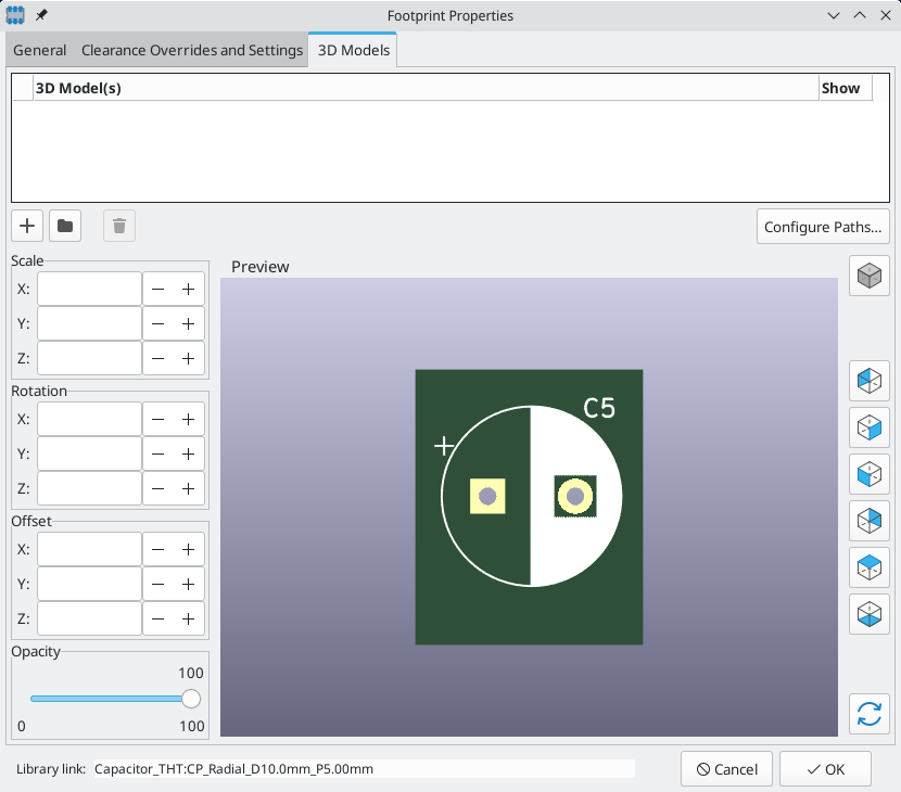
点击 ![]() 按钮,选择 IDF(*.idf;*.IDF) 文件类型筛选器。浏览到所需的边框文件。
按钮,选择 IDF(*.idf;*.IDF) 文件类型筛选器。浏览到所需的边框文件。
一旦选择了所需的元件边框文件,输入任何必要的偏移和旋转值。偏移量必须使用 IDF 板的输出单位(毫米或mil)并在 IDF 坐标系中指定,这是一个右手坐标系,+Z 指向观察者,+X 指向观察者的右边,+Y 指向屏幕的上边缘。旋转必须以度为单位;正向旋转是逆时针旋转,如 IDF v3 规范中所述。
多个边框可以与适当的偏移量结合起来,以表示简单的装配,如插座中的 DIP 封装。
| IDF 导出器只使用偏移值和 Z 旋转值,所有其他数值都被忽略。 |
创建元件边框文件
元件边框文件(*.idf)包括一个单一的 .ELECTRICAL 或 .MECHANICAL 部分,如规范文件中所述。该部分前面可以有任何数量的注释行;注释行由导出器复制到库文件中,可以用来跟踪元数据,如用于确定元件边框和尺寸的文件的参考。
元件边框部分包含字符串,整数或浮点数字段。 字符串是可包含空格的字符组合; 如果字符串包含空格,则必须引用它。 引号不得出现在字符串中。 浮点数可以使用十进制或指数表示法表示,但十进制表示法是人类可读性的首选。 小数点必须是点而不是逗号。 IDF 文件必须只包含7位 ASCII 字符; 使用8位字符将导致未定义的行为。
IDF 文件由 SECTIONS 组成,SECTIONS 由 RECORDS(记录) 组成,RECORDS 由 FIELDS(字段) 组成。对于 IDF 边框文件,只有一种类型的部分可以存在,并且必须是 .ELECTRICAL 或 .MECHANICAL 中的一种。一个记录是一行文本,可能包含一个或多个字段。字段是由一个或多个空格分隔的字符序列,不在引号之间出现。一条记录的所有字段必须出现在单行上;记录不能跨行。
Section的标题(.ELECTRICAL 或 .MECHANICAL)被认为是该节的第一条记录(记录 1)。记录 1 后面必须有记录 2,该记录有四个字段:
-
几何名称:与元件编号组合的字符串必须形成元件边框的唯一标识符。 对于标准化的封装,封装名称是几何名称的一个很好的值,例如 "SOT-23"。对于独特的封装,制造商的元件编号是几何名称的一个好选择。
-
元件编号:虽然明显是为了零件号,例如BS107,但最好使用这个字符串来帮助描述封装。 例如,如果几何名称是 "TO-92",则零件号条目可用于描述焊盘的布局或该特定 TO-92 边框文件的方向。
-
IDF 单位:必须是
MM或THOU中的一个,它只适用于描述这个单一元件边框的单位。 -
高度:这是一个浮点数,代表元件的名义高度,使用字段 3 中指定的单位。
记录 2 后面必须跟有许多记录 3 条目,这些条目指定了元件的边框。 记录 3 包含四个字段:
-
循环索引。
0(边框点按逆时针顺序指定)或1(边框点按顺时针顺序指定)。 -
X 坐标:浮点数
-
Y 坐标:浮点数
-
包括角度:一个浮点数。如果该值为
0,则从上一点到这一点绘制一条直线段。 如果数值是360,那么前一个点指定一个圆的中心,这个点指定圆上的一个点;千万不要用360的数值指定一个圆,因为至少有一个主要的机械 CAD 包在这种情况下表现不好。如果该值为负数,则从上一点到这一点将绘制顺时针方向的圆弧;如果该值为正数,则绘制逆时针方向的圆弧。
只允许一个闭环,并且无法指定切口。 指定的最后一个点必须与第一个点相同,除非边框是圆形。
示例 IDF 文件 1:
# a simple cylinder - this could represent an electrolytic capacitor
.ELECTRICAL
    "cylinder" "5mm OD, 5mm height" MM 5
    0 0 0 0
    0 2.5 0 360
.END_ELECTRICAL
示例 IDF 文件 2:
# an upside-down T
# a comment added for the sake of adding comments
.ELECTRICAL
    "Capital T" "5x8x10mm, upside down" MM 10
    0 -0.5 8 0
    0 -0.5 0.5 0
    0 -2.5 0.5 0
    0 -2.5 -0.5 180
    0 2.5 -0.5 0
    0 2.5 0.5 180
    0 0.5 0.5 0
    0 0.5 8 0
    0 -0.5 8 180
.END_ELECTRICAL
创建边框的准则
在创建边框时,特别是在与他人共享工作时,文件的设计和命名的一致性可以帮助人们更快地找到文件并以最小的麻烦放置元件。
封装命名
尽量在文件名中提供一些关于边框的信息,让用户对边框有一个大致的概念。 例如,轴向引线圆柱形封装可能代表某些类型的电容器以及某些类型的电阻,因此将边框识别为水平或垂直轴向引线器件并在相关尺寸上添加一些额外信息是有意义的:直径,长度 和间距是最重要的。 如果元件具有独特的边框,制造商的零件编号和一个前缀来表明元件的类别就足够了。
注释
使用 IDF 文件中的注释为用户提供有关边框的更多信息,例如对用于尺寸信息的源的引用。
几何形状和零件编号条目
仔细考虑要赋予几何形状和零件编号条目的值。 总之,这些字符串作为 MCAD 系统的唯一标识符。 理想情况下,字符串的值对用户有一定的意义,但这不是必需的:这些值主要用于 MCAD 系统用作唯一 ID。 理想情况下,所选择的值在任何大型边框集合中都是唯一的; 选择好的值将导致更少的冲突,特别是在复杂的电路板上。
引脚方向和定位
元件边框的创建应该与相应的封装的方向和位置相匹配。这就避免了为 IDF 元件边框指定非零旋转的需要。由于 IDF 导出器忽略了 (X,Y) 偏移值,所以在 IDF 元件边框中使用正确的原点是至关重要的。
上图显示了由程序 idfcyl 和 idfrect 生成并在一个机械 CAD 程序中渲染的样本边框。从左到右分别是 (a) 垂直径向引线圆柱体,(b) 垂直轴向引线圆柱体,左边有线路,(c) 垂直轴向引线圆柱体,右边有线路,(d) 水平轴向引线圆柱体,(e) 水平径向引线圆柱体,(f) 方形边框,普通,(g) 方形边框有倒角,(h) 方形边框有轴向引线在右边。上面的边框以毫米为单位,下面的边框以英寸为单位。
尺寸提示
拉伸边框的目的是让机械设计者了解每个元件占据的位置和物理空间。在典型情况下,机械设计师将使用更详细的机械模型替换一些粗略边框,例如在检查时确保直角安装的 LED 适合面板上的孔。在大多数情况下,边框的准确性无关紧要,但好的做法是创建可传达最佳机械信息的边框。在少数情况下,用户可能希望将元件装配到空间很小的壳体中,例如装进一个便携式音乐播放器中。在这种情况下,如果大多数拉伸边框是元件的足够好的表示,那么机械设计师可能只需要在设计壳体时替换很少的模型。如果边框不是现实的可靠反映,那么机械设计师将浪费大量时间来更换模型以确保良好的配合。毕竟,如果你把垃圾放进去,你可以预期会有垃圾出来。如果您提供了良好的信息,您可以对良好的结果充满信心。
IDF 元件边框工具
许多命令行工具可用于帮助生成 IDF 元件边框。 工具是:
-
idfcyl:创建一个垂直或水平方向的圆柱体边框,并具有轴向或径向引线 -
idfrect:创建一个矩形的边框,这个矩形可以有一个轴向引线或左上角的倒角 -
dxf2idf:将 DXF 格式的图纸转换为 IDF 元件边框
idfcyl
idfcyl 生成圆柱形元件的边框。
当 idfcyl 被调用时,没有参数,它会打印出一个使用说明和输入的摘要:
idfcyl:该程序生成圆柱形元件的边框。
     圆柱体可以是水平的或垂直的。
     水平圆柱体可以在一端或两端有导线。
     垂直圆柱体最多可以有一条导线
     放在左侧或右侧。

输入:
    单位:mm, in(毫米或英寸)
    方向:V(垂直)
    引线类型:X,R(轴向,径向)
    柱体直径
    柱体长度
    板偏移
    *   导线直径
    *   间距
    **  线侧:L,R(左,右)
    *** 引线长度
    文件名(必须以 * .idf 结尾)

    注意:
         *   仅用于水平方向或
             带轴向引线的垂直方向

        **  只有轴向引线的垂直方向才需要

        ***  仅对于带有径向引线的水平方向需要
可以通过在命令行上输入任意参数来抑制注释。 用户可以在命令行手动输入信息或创建脚本以生成边框。 以下脚本创建一个单圆柱轴向引线边框,右侧为引线:
#!/bin/bash
# Generate a cylindrical IDF outline for test purposes
# vertical 5mm cylinder,  nominal length 8mm + 3mm board offset,
# axial wire on right,  0.8mm wire dia., 3.5mm pitch
idfcyl - 1 > /dev/null <<  _EOF
mm
v
x
5
8
3
0.8
3.5
r
cylvmm_1R_D5_L8_Z3_WD0.8_P3.5.idf
_EOF
idfrect
idfrect 生成矩形元件的边框。
当 idfrect 被调用而没有参数时,它会打印出使用说明和输入摘要:
idfrect:该程序生成矩形元件的边框。
     该元件可能有有单引线(轴向)或左上角
     有倒角。
输入:
     单位:毫米,英寸(毫米或英寸)
     宽度:
     长度:
     高度:
     倒角:45 度倒角的长度
     * 引线:Y,N(引线始终向右边)
     ** 导线直径
     ** 间距
     文件名(必须以 *.idf 结尾)

    注意:
        *   仅当倒角 = 0 时才需要

        **  仅对有引线的元件有要求
可以通过在命令行上输入任意参数来抑制注释。 用户可以在命令行手动输入信息或创建脚本以生成边框。 以下脚本创建倒角矩形和轴向引线边框:
#!/bin/bash
# Generate various rectangular IDF outlines for test purposes
# 10x10, 1mm chamfer, 2mm height
idfrect - 1 > /dev/null <<  _EOF
mm
10
10
2
1
rectMM_10x10x2_C0.5.idf
_EOF
# 10x10x12,  0.8mm lead on 6mm pitch
idfrect - 1 > /dev/null <<  _EOF
mm
10
10
12
0
Y
0.8
6
rectLMM_10x10x12_D0.8_P6.0.idf
_EOF
dxf2idf
dxf2idf 从 DXF 边框创建一个 IDF 元件文件。
用于指定元件边框的 DXF 文件可以用免费软件 LibreCAD 来准备,以获得最佳的兼容性。
当 dxf2idf 被调用而没有参数时,它会打印出一个使用说明和输入的摘要:
dxf2idf:该程序从 DXF 文件中获取线段、圆弧段和圆段,并创建 IDF 元件边框文件。

输入:
     DXF 文件名:输入文件,必须以 '.dxf' 结尾
     单位:毫米,英寸(毫米或英寸)
     几何名称:字符串,根据 IDF 3.0版规范
     元件名称:根据元件号的 IDF 3.0版规范
     高度:边框的拉升高度
     注释:所有非空行都是要添加到IDF 文件
         的注释。 空行表示注释块
         结束。
     文件名:输出文件名,必须以 '.idf' 结尾
可以通过在命令行上输入任何任意参数来抑制注释的产生。用户可以在命令行上手动输入信息或创建脚本来生成边框。下面的脚本从 DXF 文件 test.dxf 创建了一个 5 毫米高的边框:
#!/bin/bash
# Generate an IDF outlines from a DXF file
dxf2idf - 1 > /dev/null << _EOF
test.dxf
mm
DXF TEST GEOMETRY
DXF TEST PART
5
This is an IDF test file produced from the outline 'test.dxf'
This is a second IDF comment to demonstrate multiple comments

test_dxf2idf.idf
_EOF
idf2vrml
idf2vrml 工具读取一组 IDF 板(.emn)和一个 IDF 元件文件(.emp)并产生一个 VRML 文件,可以用 VRML 查看器查看。在用户不能使用 MCAD 软件的情况下,这个功能对板件装配的可视化很有用。在没有任何参数的情况下调用 idf2vrml 将导致显示用发消息:
>./idf2vrml
用法: idf2vrml -f input_file.emn -s scale_factor {-k} {-d} {-z} {-d} {-z} {-m}
标志:
   -k: 产生 KiCad 友好的 VRML 输出;默认为紧凑的 VRML
   -d: 抑制对默认边框的替换
   -z: 抑制零高度边框的渲染
   -m: 打印对象映射到标准输出进行调试。
例子产生一个供 KiCad 使用的模型: idf2vrml -f input.emn -s 0.3937008 -k
idf2vrml 工具不能正确渲染 emn 文件中的 OTHER_OUTLINE 实体,如果该实体被指定在 PCB 的底层;然而你不会注意到使用 KiCad 导出的文件,因为没有机制来指定这样的实体。这如果您渲染的第三方 emn 文件确实在电路板的背面使用了实体,那么这只是一个问题。
|
操作参考
下面是 “PCB 编辑器” 中可用的 操作 的列表:可以为这些命令分配给快捷键。
PCB 编辑器
可以在 “PCB 编辑器” 中使用以下操作。可以在偏好设置中的 快捷键 部分为以下任何操作分配快捷键。
| Action | Default Hotkey | Description |
|---|---|---|
Align to Bottom |
Aligns selected items to the bottom edge |
|
Align to Horizontal Center |
Aligns selected items to the horizontal center |
|
Align to Vertical Center |
Aligns selected items to the vertical center |
|
Align to Left |
Aligns selected items to the left edge |
|
Align to Right |
Aligns selected items to the right edge |
|
Align to Top |
Aligns selected items to the top edge |
|
Distribute Horizontally |
Distributes selected items along the horizontal axis |
|
Distribute Vertically |
Distributes selected items along the vertical axis |
|
Place Off-Board Footprints |
Performs automatic placement of components outside board area |
|
Place Selected Footprints |
Performs automatic placement of selected components |
|
Flip Board View |
View board from the opposite side |
|
Sketch Graphic Items |
Show graphic items in outline mode |
|
Decrease Layer Opacity |
{ |
Make the current layer more transparent |
Increase Layer Opacity |
} |
Make the current layer less transparent |
Switch to Copper (B.Cu) Layer |
PgDn |
Switch to Copper (B.Cu) layer |
Switch to Inner Layer 1 |
Switch to Inner layer 1 |
|
Switch to Inner Layer 10 |
Switch to Inner layer 10 |
|
Switch to Inner Layer 11 |
Switch to Inner layer 11 |
|
Switch to Inner Layer 12 |
Switch to Inner layer 12 |
|
Switch to Inner Layer 13 |
Switch to Inner layer 13 |
|
Switch to Inner Layer 14 |
Switch to Inner layer 14 |
|
Switch to Inner Layer 15 |
Switch to Inner layer 15 |
|
Switch to Inner Layer 16 |
Switch to Inner layer 16 |
|
Switch to Inner Layer 17 |
Switch to Inner layer 17 |
|
Switch to Inner Layer 18 |
Switch to Inner layer 18 |
|
Switch to Inner Layer 19 |
Switch to Inner layer 19 |
|
Switch to Inner Layer 2 |
Switch to Inner layer 2 |
|
Switch to Inner Layer 20 |
Switch to Inner layer 20 |
|
Switch to Inner Layer 21 |
Switch to Inner layer 21 |
|
Switch to Inner Layer 22 |
Switch to Inner layer 22 |
|
Switch to Inner Layer 23 |
Switch to Inner layer 23 |
|
Switch to Inner Layer 24 |
Switch to Inner layer 24 |
|
Switch to Inner Layer 25 |
Switch to Inner layer 25 |
|
Switch to Inner Layer 26 |
Switch to Inner layer 26 |
|
Switch to Inner Layer 27 |
Switch to Inner layer 27 |
|
Switch to Inner Layer 28 |
Switch to Inner layer 28 |
|
Switch to Inner Layer 29 |
Switch to Inner layer 29 |
|
Switch to Inner Layer 3 |
Switch to Inner layer 3 |
|
Switch to Inner Layer 30 |
Switch to Inner layer 30 |
|
Switch to Inner Layer 4 |
Switch to Inner layer 4 |
|
Switch to Inner Layer 5 |
Switch to Inner layer 5 |
|
Switch to Inner Layer 6 |
Switch to Inner layer 6 |
|
Switch to Inner Layer 7 |
Switch to Inner layer 7 |
|
Switch to Inner Layer 8 |
Switch to Inner layer 8 |
|
Switch to Inner Layer 9 |
Switch to Inner layer 9 |
|
Switch to Next Layer |
+ |
Switch to Next Layer |
Switch to Previous Layer |
- |
Switch to Previous Layer |
Toggle Layer |
V |
Switch between layers in active layer pair |
Switch to Component (F.Cu) layer |
PgUp |
Switch to Component (F.Cu) layer |
Net Inspector |
Show the net inspector |
|
Local Ratsnest |
Toggle ratsnest display of selected item(s) |
|
Net Color Mode (3-state) |
Cycle between using net and netclass colors for all nets, just ratsnests, and none |
|
Sketch Pads |
Show pads in outline mode |
|
Curved Ratsnest Lines |
Show ratsnest with curved lines |
|
Ratsnest Mode (3-state) |
Cycle between showing ratsnests for all layers, just visible layers, and none |
|
Repair Board |
Run various diagnostics and attempt to repair board |
|
Show Appearance Manager |
Show/hide the appearance manager |
|
Show Pad Numbers |
Show pad numbers |
|
Scripting Console |
Show the Python scripting console |
|
Show Ratsnest |
Show board ratsnest |
|
Sketch Text Items |
Show footprint texts in line mode |
|
Sketch Tracks |
K |
Show tracks in outline mode |
Sketch Vias |
Show vias in outline mode |
|
Draw Zone Outlines |
Show only zone boundaries |
|
Draw Zone Fills |
Show filled areas of zones |
|
Toggle Zone Display |
Cycle between showing zone fills and just their outlines |
|
Create Arc from Selection |
Creates an arc from the selected line segment |
|
Create Rule Area from Selection… |
Creates a rule area from the selection |
|
Create Lines from Selection… |
Creates graphic lines from the selection |
|
Create Polygon from Selection… |
Creates a graphic polygon from the selection |
|
Create Tracks from Selection |
Creates tracks from the selected graphic lines |
|
Create Zone from Selection… |
Creates a copper zone from the selection |
|
Design Rules Checker |
Show the design rules checker window |
|
Open in Footprint Editor |
Ctrl+E |
Opens the selected footprint in the Footprint Editor |
Edit Library Footprint… |
Ctrl+Shift+E |
Opens the selected footprint in the Footprint Editor |
Append Board… |
Open another board and append its contents to this board |
|
Assign Netclass… |
Assign a netclass to nets matching a pattern |
|
Board Setup… |
Edit board setup including layers, design rules and various defaults |
|
Clear Net Highlighting |
~ |
Clear any existing net highlighting |
Drill/Place File Origin |
Place origin point for drill files and component placement files |
|
Reset Drill Origin |
||
Export Specctra DSN… |
Export Specctra DSN routing info |
|
Bill of Materials… |
Create bill of materials from board |
|
IPC-D-356 Netlist File… |
Generate IPC-D-356 netlist file |
|
Drill Files (.drl)… |
Generate Excellon drill file(s) |
|
Gerbers (.gbr)… |
Generate Gerbers for fabrication |
|
IPC-2581 File (.xml)… |
Generate an IPC-2581 file |
|
Component Placement (.pos, .gbr)… |
Generate component placement file(s) for pick and place |
|
Footprint Report (.rpt)… |
Create report of all footprints from current board |
|
Group Items |
Group the selected items so that they are treated as a single item |
|
Enter Group |
Enter the group to edit items |
|
Leave Group |
Leave the current group |
|
Hide Net in Ratsnest |
Hide the selected net in the ratsnest of unconnected net lines/arcs |
|
Highlight Net |
` |
Highlight net under cursor |
Highlight Net |
Highlight all copper items on the selected net(s) |
|
Import Netlist… |
Read netlist and update board connectivity |
|
Import Specctra Session… |
Import routed Specctra session (*.ses) file |
|
Lock |
Prevent items from being moved and/or resized on the canvas |
|
Add Footprint |
A |
Add a footprint |
Remove Items |
Remove items from group |
|
Switch to Schematic Editor |
Open schematic in schematic editor |
|
Show Net in Ratsnest |
Show the selected net in the ratsnest of unconnected net lines/arcs |
|
Constrain to H, V, 45 |
Shift+Space |
Limit actions to horizontal, vertical, or 45 degrees from the starting point |
Toggle Last Net Highlight |
Toggle between last two highlighted nets |
|
Toggle Lock |
L |
Lock or unlock selected items |
Toggle Net Highlight |
Alt+` |
Toggle net highlighting |
Switch Track Width to Previous |
Shift+W |
Change track width to previous pre-defined size |
Switch Track Width to Next |
W |
Change track width to next pre-defined size |
Ungroup Items |
Ungroup any selected groups |
|
Unlock |
Allow items to be moved and/or resized on the canvas |
|
Decrease Via Size |
kbd:[\] |
Change via size to previous pre-defined size |
Increase Via Size |
' |
Change via size to next pre-defined size |
Duplicate Zone onto Layer… |
Duplicate zone outline onto a different layer |
|
Merge Zones |
Merge zones |
|
Rebuild All Generators |
Rebuilds geometry of all generators |
|
Update All Tuning Patterns |
Attempt to re-tune existing tuning patterns within their bounds |
|
Rebuild Selected Generators |
Rebuilds geometry of selected generator(s) |
|
Generators Manager |
Show a manager dialog for Generator objects |
|
Change Footprint… |
Assign a different footprint from the library |
|
Change Footprints… |
Assign different footprints from the library |
|
Cleanup Graphics… |
Cleanup redundant items, etc. |
|
Cleanup Tracks & Vias… |
Cleanup redundant items, shorting items, etc. |
|
Edit Teardrops… |
Add, remove or edit teardrops globally across board |
|
Edit Text & Graphics Properties… |
Edit Text and graphics properties globally across board |
|
Edit Track & Via Properties… |
Edit track and via properties globally across board |
|
Global Deletions… |
Delete tracks, footprints and graphic items from board |
|
Remove Unused Pads… |
Remove or restore the unconnected inner layers on through hole pads and vias |
|
Swap Layers… |
Move tracks or drawings from one layer to another |
|
Update Footprint… |
Update footprint to include any changes from the library |
|
Update Footprints from Library… |
Update footprints to include any changes from the library |
|
Compare Footprint with Library |
Show differences between board footprint and its library equivalent |
|
Clearance Resolution |
Show clearance resolution for the active layer between two selected objects |
|
Constraints Resolution |
Show constraints resolution for the selected object |
|
Show Board Statistics |
Shows board statistics |
|
Show Footprint Associations |
Show footprint library and schematic symbol associations |
|
Add Aligned Dimension |
Ctrl+Shift+H |
Add an aligned linear dimension |
Draw Arc |
Ctrl+Shift+A |
Draw an arc |
Switch Arc Posture |
/ |
Switch the arc posture |
Add Center Dimension |
Add a center dimension |
|
Draw Circle |
Ctrl+Shift+C |
Draw a circle |
Close Outline |
Close the in progress outline |
|
Decrease Line Width |
Ctrl+- |
Decrease the line width |
Delete Last Point |
Back |
Delete the last point added to the current item |
Draw Graphic Polygon |
Ctrl+Shift+P |
Draw a graphic polygon |
Increase Line Width |
Ctrl++ |
Increase the line width |
Add Leader |
Add a leader dimension |
|
Draw Line |
Ctrl+Shift+L |
Draw a line |
Add Orthogonal Dimension |
Add an orthogonal dimension |
|
Add Board Characteristics |
Add a board characteristics table on a graphic layer |
|
Import Graphics… |
Ctrl+Shift+F |
Import 2D drawing file |
Add Reference Image |
Add a bitmap image to be used as a reference (image will not be included in any output) |
|
Add Stackup Table |
Add a board stackup table on a graphic layer |
|
Add Radial Dimension |
Add a radial dimension |
|
Draw Rectangle |
Draw a rectangle |
|
Add Rule Area |
Ctrl+Shift+K |
Add a rule area (keepout) |
Place the Footprint Anchor |
Ctrl+Shift+N |
Set the coordinate origin point (anchor) of the footprint |
Add a Similar Zone |
Ctrl+Shift+. |
Add a zone with the same settings as an existing zone |
Add Text |
Ctrl+Shift+T |
Add a text item |
Add Text Box |
Add a wrapped text item |
|
Add Vias |
Ctrl+Shift+V |
Add free-standing vias |
Add Filled Zone |
Ctrl+Shift+Z |
Add a filled zone |
Add a Zone Cutout |
Shift+C |
Add a cutout area of an existing zone |
Get and Move Footprint |
T |
Selects a footprint by reference designator and places it under the cursor for moving |
Chamfer Lines |
Cut away corners between selected lines |
|
Change Track Width |
Updates selected track & via sizes |
|
Create Array… |
Ctrl+T |
Create array |
Delete Full Track |
Shift+Del |
Deletes selected item(s) and copper connections |
Duplicate and Increment |
Ctrl+Shift+D |
Duplicates the selected item(s), incrementing pad numbers |
Extend Lines to Meet |
Extend lines to meet each other |
|
Fillet Lines… |
Adds arcs tangent to the selected lines |
|
Fillet Tracks |
Adds arcs tangent to the selected straight track segments |
|
Change Side / Flip |
F |
Flips selected item(s) to opposite side of board |
Heal Shapes |
Connect shapes, possibly extending or cutting them, or adding extra geometry |
|
Intersect Polygons |
Create the intersection of the selected polygons |
|
Merge Polygons |
Merge selected polygons into a single polygon |
|
Mirror Horizontally |
Mirrors selected item across the Y axis |
|
Mirror Vertically |
Mirrors selected item across the X axis |
|
Move Corner To… |
Move the active corner to an exact location |
|
Move Exactly… |
Shift+M |
Moves the selected item(s) by an exact amount |
Move Midpoint To… |
Move the active midpoint to an exact location |
|
Pack and Move Footprints |
P |
Sorts selected footprints by reference, packs based on size and initiates movement |
Properties… |
E |
Displays item properties dialog |
Rotate Counterclockwise |
R |
Rotates selected item(s) counterclockwise |
Rotate Clockwise |
Shift+R |
Rotates selected item(s) clockwise |
Skip |
Tab |
Skip item |
Subtract Polygons |
Subtract selected polygons from the last one selected |
|
Swap |
S |
Swaps selected items' positions |
Copy with Reference |
Copy selected item(s) to clipboard with a specified starting point |
|
Move |
M |
Moves the selected item(s) |
Move Individually |
Ctrl+M |
Moves the selected items one-by-one |
Move with Reference |
Moves the selected item(s) with a specified starting point |
|
Attempt Finish |
F |
Attempts to complete current route to nearest ratsnest end. |
Attempt Finish Selected (Autoroute) |
Shift+F |
Sequentially attempt to automatically route all selected pads. |
Break Track |
Splits the track segment into two segments connected at the cursor position. |
|
Route From Other End |
Ctrl+E |
Commits current segments and starts next segment from nearest ratsnest end. |
Custom Track/Via Size… |
Q |
Shows a dialog for changing the track width and via size. |
Cycle Router Mode |
Cycle router to the next mode |
|
Route Differential Pair |
6 |
Route differential pairs |
Differential Pair Dimensions… |
Open Differential Pair Dimension settings |
|
Drag 45 Degree Mode |
D |
Drags the track segment while keeping connected tracks at 45 degrees. |
Drag Free Angle |
G |
Drags the nearest joint in the track without restricting the track angle. |
Router Highlight Mode |
Switch router to highlight mode |
|
Place Blind/Buried Via |
Alt+Shift+V |
Adds a blind or buried via at the end of currently routed track. |
Place Microvia |
Ctrl+V |
Adds a microvia at the end of currently routed track. |
Place Through Via |
V |
Adds a through-hole via at the end of currently routed track. |
Route Selected |
Shift+X |
Sequentially route selected items from ratsnest anchor. |
Route Selected From Other End |
Shift+E |
Sequentially route selected items from other end of ratsnest anchor. |
Select Layer and Place Blind/Buried Via… |
Alt+< |
Select a layer, then add a blind or buried via at the end of currently routed track. |
Select Layer and Place Micro Via… |
Select a layer, then add a micro via at the end of currently routed track. |
|
Select Layer and Place Through Via… |
< |
Select a layer, then add a through-hole via at the end of currently routed track. |
Set Layer Pair… |
Change active layer pair for routing |
|
Interactive Router Settings… |
Ctrl+< |
Open Interactive Router settings |
Router Shove Mode |
Switch router to shove mode |
|
Route Single Track |
X |
Route tracks |
Switch Track Posture |
/ |
Switches posture of the currently routed track. |
Track Corner Mode |
Ctrl+/ |
Switches between sharp/rounded and 45°/90° corners when routing tracks. |
Undo Last Segment |
Back |
Walks the current track back one segment. |
Router Walkaround Mode |
Switch router to walkaround mode |
|
Deselect All Tracks in Net |
Deselects all tracks & vias belonging to the same net. |
|
Filter Selected Items… |
Remove items from the selection by type |
|
Grab Nearest Unconnected Footprints |
Shift+O |
Selects and initiates moving the nearest unconnected footprint on each selected net. |
Select/Expand Connection |
U |
Selects a connection or expands an existing selection to junctions, pads, or entire connections |
Select All Tracks in Net |
Selects all tracks & vias belonging to the same net. |
|
Select on Schematic |
Selects corresponding items in Schematic editor |
|
Sheet |
Selects all footprints and tracks in the schematic sheet |
|
Items in Same Hierarchical Sheet |
Selects all footprints and tracks in the same schematic sheet |
|
Select All Unconnected Footprints |
O |
Selects all unconnected footprints belonging to each selected net. |
Unroute Selected |
Unroutes selected items to the nearest pad. |
|
Tune Skew of a Differential Pair |
9 |
Tune skew of a differential pair |
Tune Length |
7 |
Tune length of a single track or differential pair |
Add Microwave Polygonal Shape |
Create a microwave polygonal shape from a list of vertices |
|
Add Microwave Gap |
Create gap of specified length for microwave applications |
|
Add Microwave Line |
Create line of specified length for microwave applications |
|
Add Microwave Stub |
Create stub of specified length for microwave applications |
|
Add Microwave Arc Stub |
Create stub (arc) of specified size for microwave applications |
|
Footprint Checker |
Show the footprint checker window |
|
Copy Footprint |
Copy Footprint |
|
Create Footprint… |
Create a new footprint using the Footprint Wizard |
|
Cut Footprint |
Cut Footprint |
|
Delete Footprint from Library |
Delete Footprint from Library |
|
Duplicate Footprint |
Make a copy of the selected footprint |
|
Edit Footprint |
Show selected footprint on editor canvas |
|
Export Current Footprint… |
Export edited footprint to file |
|
Footprint Properties… |
Edit footprint properties |
|
Hide Footprint Tree |
Hide Footprint Tree |
|
Import Footprint… |
Import footprint from file |
|
New Footprint… |
Ctrl+N |
Create a new, empty footprint |
Paste Footprint |
Paste Footprint |
|
Rename Footprint… |
Rename the selected footprint |
|
Repair Footprint |
Run various diagnostics and attempt to repair footprint |
|
Show Footprint Tree |
Show Footprint Tree |
|
Paste Default Pad Properties to Selected |
Replace the current pad’s properties with those copied earlier |
|
Copy Pad Properties to Default |
Copy current pad’s properties |
|
Push Pad Properties to Other Pads… |
Copy the current pad’s properties to other pads |
|
Default Pad Properties… |
Edit the pad properties used when creating new pads |
|
Renumber Pads… |
Renumber pads by clicking on them in the desired order |
|
Edit Pad as Graphic Shapes |
Ctrl+E |
Ungroups a custom-shaped pad for editing as individual graphic shapes |
Add Pad |
Add a pad |
|
Finish Pad Edit |
Ctrl+E |
Regroups all touching graphic shapes into the edited pad |
Create Corner |
Ins |
Create a corner |
Keep Arc Center, Adjust Radius |
Switch arc editing mode to keep center, adjust radius and endpoints |
|
Keep Arc Endpoints or Direction of Starting Point |
Switch arc editing mode to keep endpoints, or to keep direction of the other point |
|
Remove Corner |
Remove corner |
|
Position Relative To… |
Shift+P |
Positions the selected item(s) by an exact amount relative to another |
Geographical Reannotate… |
Reannotate PCB in geographical order |
|
Refresh Plugins |
Reload all python plugins and refresh plugin menus |
|
Open Plugin Directory |
Opens the directory in the default system file manager |
|
Draft Fill Selected Zone(s) |
Update copper fill of selected zone(s) without regard to other interacting zones |
|
Fill All Zones |
B |
Update copper fill of all zones |
Unfill Selected Zone(s) |
Remove copper fill from selected zone(s) |
|
Unfill All Zones |
Ctrl+B |
Remove copper fill from all zones |
Decrease Amplitude |
4 |
Decrease tuning pattern amplitude by one step. |
Increase Amplitude |
3 |
Increase tuning pattern amplitude by one step. |
Decrease Spacing |
2 |
Decrease tuning pattern spacing by one step. |
Increase Spacing |
1 |
Increase tuning pattern spacing by one step. |
3D 查看器
以下动作可在 3D 浏览器中使用。快捷键可以分配给偏好设置中的 快捷键 部分的任何这些操作。
| Action | Default Hotkey | Description |
|---|---|---|
Show 3D Models marked DNP |
D |
Show 3D models even if marked 'Do Not Place' |
Show 3D Models not in POS File |
P |
Show 3D models even if not found in .pos file |
Show Unspecified 3D Models |
V |
Show 3D models for 'unspecified' type footprints |
Show SMD 3D Models |
S |
Show 3D models for 'Surface mount' type footprints |
Show Through Hole 3D Models |
T |
Show 3D models for 'Through hole' type footprints |
Flip Board |
F |
Flip the board view |
Home View |
Home |
Home view |
Render CAD Colors |
Use a CAD color style based on the diffuse color of the material |
|
Render Solid Colors |
Use only the diffuse color property from 3D model file |
|
Render Realistic Materials |
Use all material properties from each 3D model file |
|
Move Board Down |
Down |
Move board Down |
Move Board Left |
Left |
Move board Left |
Move Board Right |
Right |
Move board Right |
Move Board Up |
Up |
Move board Up |
No 3D Grid |
No 3D Grid |
|
Set Pivot |
Space |
Place point around which the board will be rotated (middle mouse click) |
Rotate X Clockwise |
Rotate X Clockwise |
|
Rotate X Counterclockwise |
Rotate X Counterclockwise |
|
Rotate Y Clockwise |
Rotate Y Clockwise |
|
Rotate Y Counterclockwise |
Rotate Y Counterclockwise |
|
Rotate Z Clockwise |
Rotate Z Clockwise |
|
Rotate Z Counterclockwise |
Rotate Z Counterclockwise |
|
3D Grid 10mm |
3D Grid 10mm |
|
3D Grid 1mm |
3D Grid 1mm |
|
3D Grid 2.5mm |
3D Grid 2.5mm |
|
3D Grid 5mm |
3D Grid 5mm |
|
Show 3D Axis |
Show 3D Axis |
|
Show Model Bounding Boxes |
Show 3D model bounding boxes in realtime renderer |
|
Show Appearance Manager |
Show/hide the appearance manager |
|
Toggle Orthographic Projection |
Enable/disable orthographic projection |
|
View Back |
Shift+Y |
View Back |
View Bottom |
Shift+Z |
View Bottom |
View Front |
Y |
View Front |
View Left |
Shift+X |
View Left |
View Right |
X |
View Right |
View Top |
Z |
View Top |
通用
以下操作在整个 KiCad 中都可用,包括在 PCB 编辑器中。快捷键可以分配给偏好设置中的 快捷键 部分的任何操作。
| Action | Default Hotkey | Description |
|---|---|---|
Exclude Marker |
Mark current violation in Checker window as an exclusion |
|
Next Marker |
Go to next marker in Checker window |
|
Previous Marker |
Go to previous marker in Checker window |
|
Add Library… |
Add an existing library folder |
|
Click |
Return |
Performs left mouse button click |
Double-click |
End |
Performs left mouse button double-click |
Cursor Down |
Down |
|
Cursor Down Fast |
Ctrl+Down |
|
Cursor Left |
Left |
|
Cursor Left Fast |
Ctrl+Left |
|
Cursor Right |
Right |
|
Cursor Right Fast |
Ctrl+Right |
|
Cursor Up |
Up |
|
Cursor Up Fast |
Ctrl+Up |
|
Grid Origin… |
Set the grid origin point |
|
Edit Grids… |
Edit grid definitions |
|
Switch to Fast Grid 1 |
Alt+1 |
|
Switch to Fast Grid 2 |
Alt+2 |
|
Cycle Fast Grid |
Alt+4 |
|
Switch to Next Grid |
N |
|
Switch to Previous Grid |
Shift+N |
|
Reset Grid Origin |
||
Grid Origin |
Place the grid origin point |
|
Inactive Layer View Mode |
Toggle inactive layers between normal and dimmed |
|
Inactive Layer View Mode (3-state) |
H |
Cycle inactive layers between normal, dimmed, and hidden |
Inches |
Use inches |
|
Snap to Objects on the Active Layer Only |
Enables snapping to objects on the active layer only |
|
Snap to Objects on All Layers |
Enables snapping to objects on all visible layers |
|
Toggle Snapping Between Active and All Layers |
Shift+S |
Toggles between snapping on all visible layers and only the active area |
Millimeters |
Use millimeters |
|
Mils |
Use mils |
|
New… |
Ctrl+N |
Create a new document in the editor |
New Library… |
Create a new library folder |
|
Open… |
Ctrl+O |
Open existing document |
Page Settings… |
Settings for paper size and title block info |
|
Pan Down |
Shift+Down |
|
Pan Left |
Shift+Left |
|
Pan Right |
Shift+Right |
|
Pan Up |
Shift+Up |
|
Pin Library |
Keep the library at the top of the list |
|
Plot… |
Plot |
|
Print… |
Ctrl+P |
|
Quit |
Close the current editor |
|
Redo Last Zoom |
Return zoom to level prior to last zoom undo |
|
Reset Local Coordinates |
Space |
|
Revert |
Throw away changes |
|
Save |
Ctrl+S |
Save changes |
Save All |
Save all changes |
|
Save As… |
Ctrl+Shift+S |
Save current document to another location |
Save a Copy… |
Save a copy of the current document to another location |
|
Select Columns… |
||
3D Viewer |
Alt+3 |
Show 3D viewer window |
Show Context Menu |
Perform the right-mouse-button action |
|
Footprint Library Browser |
Browse footprint libraries |
|
Footprint Editor |
Create, delete and edit footprints |
|
Switch to Project Manager |
Show project window |
|
Show Properties Manager |
Show/hide the properties manager |
|
Symbol Library Browser |
Browse symbol libraries |
|
Symbol Editor |
Create, delete and edit symbols |
|
Draw Bounding Boxes |
Draw Bounding Boxes |
|
Always Show Cursor |
Ctrl+Shift+X |
Display crosshairs even in selection tool |
Full-Window Crosshairs |
Switch display of full-window crosshairs |
|
Show Grid |
Display background grid in the edit window |
|
Grid Overrides |
Ctrl+Shift+G |
Enables item-specific grids that override the current grid |
Polar Coordinates |
Switch between polar and cartesian coordinate systems |
|
Switch units |
Ctrl+U |
Switch between imperial and metric units |
Undo Last Zoom |
Return zoom to level prior to last zoom action |
|
Unpin Library |
No longer keep the library at the top of the list |
|
Update PCB from Schematic… |
F8 |
Update PCB with changes made to schematic |
Update Schematic from PCB… |
Update schematic with changes made to PCB |
|
Center on Cursor |
F4 |
Center on Cursor |
Zoom to Objects |
Ctrl+Home |
Zoom to Objects |
Zoom to Fit |
Home |
Zoom to Fit |
Zoom In at Cursor |
F1 |
Zoom In at Cursor |
Zoom In |
Zoom In |
|
Zoom Out at Cursor |
F2 |
Zoom Out at Cursor |
Zoom Out |
Zoom Out |
|
Refresh |
F5 |
Refresh |
Zoom to Selection |
Ctrl+F5 |
Zoom to Selection |
Cancel |
Cancel current tool |
|
Copy |
Ctrl+C |
Copy selected item(s) to clipboard |
Cut |
Ctrl+X |
Cut selected item(s) to clipboard |
Cycle Arc Editing Mode |
Ctrl+Space |
Switch to a different method of editing arcs |
Delete |
Del |
Deletes selected item(s) |
Interactive Delete Tool |
Delete clicked items |
|
Duplicate |
Ctrl+D |
Duplicates the selected item(s) |
Find |
Ctrl+F |
Find text |
Find and Replace |
Ctrl+Alt+F |
Find and replace text |
Find Next |
F3 |
Find next match |
Find Next Marker |
Ctrl+Shift+F3 |
|
Find Previous |
Shift+F3 |
Find previous match |
Finish |
End |
Finish current tool |
Paste |
Ctrl+V |
Paste item(s) from clipboard |
Paste Special… |
Paste item(s) from clipboard with annotation options |
|
Redo |
Ctrl+Y |
Redo last edit |
Replace All |
Replace all matches |
|
Replace and Find Next |
Replace current match and find next |
|
Show Search Panel |
Ctrl+G |
Show/hide the search panel |
Select All |
Ctrl+A |
Select all items on screen |
Undo |
Ctrl+Z |
Undo last edit |
Unselect All |
Ctrl+Shift+A |
Unselect all items on screen |
Measure Tool |
Ctrl+Shift+M |
Interactively measure distance between points |
Select item(s) |
Select item(s) |
|
About KiCad |
Open about dialog |
|
Configure Paths… |
Edit path configuration environment variables |
|
Donate |
Open "Donate to KiCad" in a web browser |
|
Get Involved |
Open "Contribute to KiCad" in a web browser |
|
Getting Started with KiCad |
Open “Getting Started in KiCad” guide for beginners |
|
Help |
Open product documentation in a web browser |
|
List Hotkeys… |
Ctrl+F1 |
Displays current hotkeys table and corresponding commands |
Preferences… |
Ctrl+, |
Show preferences for all open tools |
Report Bug |
Report a problem with KiCad |
|
Manage Footprint Libraries… |
Edit the global and project footprint library lists |
|
Manage Symbol Libraries… |
Edit the global and project symbol library lists |